- 您現(xiàn)在的位置:買賣IC網(wǎng) > PDF目錄385416 > HY29LV160TF-80 (HYNIX SEMICONDUCTOR INC) 16 Mbit (2M x 8/1M x 16) Low Voltage Flash Memory PDF資料下載
參數(shù)資料
| 型號: | HY29LV160TF-80 |
| 廠商: | HYNIX SEMICONDUCTOR INC |
| 元件分類: | DRAM |
| 英文描述: | 16 Mbit (2M x 8/1M x 16) Low Voltage Flash Memory |
| 中文描述: | 1M X 16 FLASH 2.7V PROM, 80 ns, PBGA48 |
| 封裝: | 8 X 9 MM, FBGA-48 |
| 文件頁數(shù): | 15/48頁 |
| 文件大小: | 517K |
| 代理商: | HY29LV160TF-80 |
第1頁第2頁第3頁第4頁第5頁第6頁第7頁第8頁第9頁第10頁第11頁第12頁第13頁第14頁當(dāng)前第15頁第16頁第17頁第18頁第19頁第20頁第21頁第22頁第23頁第24頁第25頁第26頁第27頁第28頁第29頁第30頁第31頁第32頁第33頁第34頁第35頁第36頁第37頁第38頁第39頁第40頁第41頁第42頁第43頁第44頁第45頁第46頁第47頁第48頁
15
Rev. 1.2/May 01
HY29LV160
Chip Erase Command
The Chip Erase command sequence consists of
two unlock cycles, followed by a set-up command,
two additional unlock cycles and then the Chip
Erase command. This sequence invokes the Au-
tomatic Erase algorithm which automatically
preprograms and verifies the entire memory for
an all zero data pattern prior to electrical erase.
The host system is not required to provide any
controls or timings during these operations.
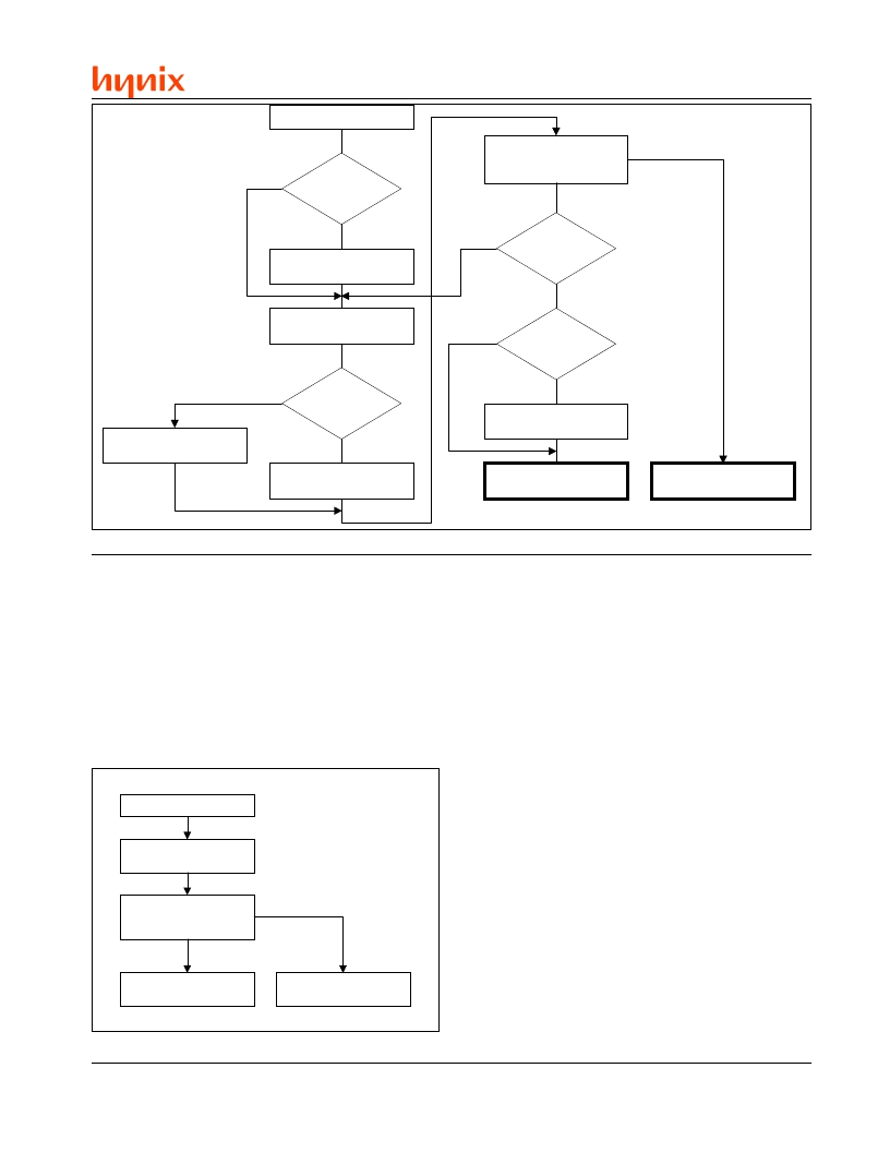
Figure 4. Normal and Unlock Bypass Programming Procedures
Figure 5. Chip Erase Procedure
START
Issue CHIP ERASE
Command Sequence
Check Erase Status
(See Write Operation Status
Section)
CHIP ERASE COMPLETE
GO TO
ERROR RECOVERY
DQ[5] Error Exit
Normal Exit
Commands written to the device during execution
of the Automatic Erase algorithm are ignored. Note
that a hardware reset immediately terminates the
chip erase operation. To ensure data integrity,
the aborted Chip Erase command sequence
should be reissued once the reset operation is
complete.
When the Automatic Erase algorithm is complete,
the device returns to the array Read mode. Sev-
eral methods are provided to allow the host to
determine the status of the erase operation, as
described in the Write Operation Status section.
Figure 5 illustrates the chip erase procedure.
Sector Erase Command
The Sector Erase command sequence consists
of two unlock cycles, followed by the Erase com-
mand, two additional unlock cycles and then the
sector erase data cycle, which specifies the sec-
tor to be erased. As described later in this sec-
tion, multiple sectors can be specified for erasure
with a single command sequence. During sector
erase, all specified sectors are erased sequen-
tially. The data in sectors not specified for era-
sure, as well as the data in any protected sectors,
START
Enable Fast
Programming
Issue UNLOCK BYPASS
Command
YES
NO
Unlock Bypass
Mode
Issue UNLOCK BYPASS
PROGRAM Command
Issue NORMAL PROGRAM
Command
Check Programming Status
(See Write Operation Status
Section)
YES
NO
Last Word/Byte
Done
YES
NO
Setup Next Address/Data for
Program Operation
YES
NO
Unlock Bypass
Mode
Issue UNLOCK BYPASS
RESET Command
PROGRAMMING
COMPLETE
GO TO ERROR
RECOVERY PROCEDURE
DQ[5] Error Exit
Programming Verified
相關(guān)PDF資料 |
PDF描述 |
|---|---|
| HY29LV160BF-90 | 16 Mbit (2M x 8/1M x 16) Low Voltage Flash Memory |
| HY29LV160TF-90 | 16 Mbit (2M x 8/1M x 16) Low Voltage Flash Memory |
| HY29LV160BF-70I | 16 Mbit (2M x 8/1M x 16) Low Voltage Flash Memory |
| HY29LV160BF-80I | 16 Mbit (2M x 8/1M x 16) Low Voltage Flash Memory |
| HY29LV160BF-90I | ECONOLINE: RKZ - Safety standards and approvals: EN 60950 certified, rated for 250VAC (LVD test report)- Custom Solutions Available- 3kVDC & 4kVDC Isolation- UL94V-0 Package Material- Power Sharing on Output- Efficiency to 84% |
相關(guān)代理商/技術(shù)參數(shù) |
參數(shù)描述 |
|---|---|
| HY29LV160TF-80I | 制造商:HYNIX 制造商全稱:Hynix Semiconductor 功能描述:16 Mbit (2M x 8/1M x 16) Low Voltage Flash Memory |
| HY29LV160TF-90 | 制造商:HYNIX 制造商全稱:Hynix Semiconductor 功能描述:16 Mbit (2M x 8/1M x 16) Low Voltage Flash Memory |
| HY29LV160TF-90I | 制造商:HYNIX 制造商全稱:Hynix Semiconductor 功能描述:16 Mbit (2M x 8/1M x 16) Low Voltage Flash Memory |
| HY29LV160TT-12 | 制造商:HYNIX 制造商全稱:Hynix Semiconductor 功能描述:16 Mbit (2M x 8/1M x 16) Low Voltage Flash Memory |
| HY29LV160TT-12I | 制造商:HYNIX 制造商全稱:Hynix Semiconductor 功能描述:16 Mbit (2M x 8/1M x 16) Low Voltage Flash Memory |
發(fā)布緊急采購,3分鐘左右您將得到回復(fù)。