- 您現(xiàn)在的位置:買賣IC網(wǎng) > PDF目錄296200 > HYB39S64160AT-6 (INFINEON TECHNOLOGIES AG) 4M X 16 SYNCHRONOUS DRAM, 5 ns, PDSO54 PDF資料下載
參數(shù)資料
| 型號: | HYB39S64160AT-6 |
| 廠商: | INFINEON TECHNOLOGIES AG |
| 元件分類: | DRAM |
| 英文描述: | 4M X 16 SYNCHRONOUS DRAM, 5 ns, PDSO54 |
| 封裝: | 10.16 X 22.22 MM, 0.80 MM PITCH, PLASTIC, TSOP2-54 |
| 文件頁數(shù): | 3/18頁 |
| 文件大小: | 118K |
| 代理商: | HYB39S64160AT-6 |
INFINEON Technologies
11
HYB39S6416A/BT-5.5/-6/-7
64MBit Synchronous DRAM
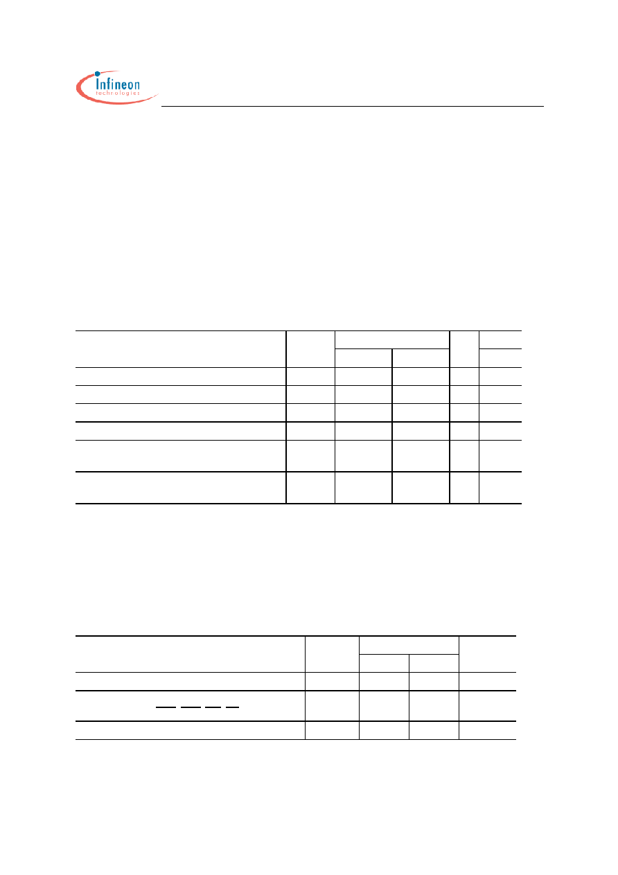
Absolute Maximum Ratings
Operating temperature range......................................................................................... 0 to + 70
°C
Storage temperature range..................................................................................... – 55 to + 150
°C
Input/output voltage .............................................................................. – 0.5 to min(Vcc+0.5, 4.6) V
Power supply voltage VDD / VDDQ.......................................................................... – 1.0 to + 4.6 V
Power Dissipation............................................. ..........................................................................1 W
Data out current (short circuit) ................................................................................................ 50 mA
Note:
Stresses above those listed under “Absolute Maximum Ratings” may cause permanent
damage of the device. Exposure to absolute maximum rating conditions for extended periods
may affect device reliability.
Recommended Operation and Characteristics :
T
A = 0 to 70 °C; VSS = 0 V; VDD,VDDQ = 3.3 V ± 0.3 V
Notes:
1. All voltages are referenced to VSS.
2. Vih may overshoot to Vdd + 2.0 V for pulse width of < 4ns with 3.3V. Vil may undershoot to
-2.0 V for pulse width < 4.0 ns with 3.3V. Pulse width measured at 50% points with amplitude measured peak
to DC reference.
Capacitance
T
A = 0 to 70 °C; VDD = 3.3 V ± 0.3 V, f = 1 MHz
Parameter
Symbol
Limit Values
Unit Notes
min.
max.
Input high voltage
V
IH
2.0
Vdd+0.3
V
1, 2
Input low voltage
V
IL
– 0.3
0.8
V
1, 2
Output high voltage (
I
OUT = – 4.0 mA)
V
OH
2.4
–
V
Output low voltage (
I
OUT =4.0 mA)
V
OL
–0.4
V
Input leakage current, any input
(0 V <
V
IN < Vddq, all other inputs = 0 V)
I
I(L)
– 5
5
A
Output leakage current
(DQ is disabled, 0 V <
V
OUT < Vdd)
I
O(L)
– 5
5
A
Parameter
Symbol
Values
Unit
min.
max.
Input capacitance (CLK)
C
I1
2.5
3.5
pF
Input capacitance
(A0-A12, BA0,BA1,RAS, CAS, WE, CS, CKE, DQM)
C
I2
2.5
3.8
pF
Input / Output capacitance (DQ)
C
IO
4.0
6.0
pF
相關(guān)PDF資料 |
PDF描述 |
|---|---|
| HYB39T256160TT-5 | MEMORY SPECTRUM |
| HYB39T256160TT-6 | MEMORY SPECTRUM |
| HYB39T256160TT-7 | MEMORY SPECTRUM |
| HYB39T256160TT-75 | MEMORY SPECTRUM |
| HYB39T256160TT-7F | MEMORY SPECTRUM |
相關(guān)代理商/技術(shù)參數(shù) |
參數(shù)描述 |
|---|---|
| HYB39S64160AT-7 | 制造商:未知廠家 制造商全稱:未知廠家 功能描述:x16 SDRAM |
| HYB39S64160AT-7.5 | 制造商:未知廠家 制造商全稱:未知廠家 功能描述:x16 SDRAM |
| HYB39S64160AT-8 | 制造商:INFINEON 制造商全稱:Infineon Technologies AG 功能描述:64 MBit Synchronous DRAM |
| HYB39S64160AT-8B | 制造商:INFINEON 制造商全稱:Infineon Technologies AG 功能描述:64 MBit Synchronous DRAM |
| HYB39S64160ATL-10 | 制造商:未知廠家 制造商全稱:未知廠家 功能描述:x16 SDRAM |
發(fā)布緊急采購,3分鐘左右您將得到回復(fù)。