- 您現(xiàn)在的位置:買賣IC網(wǎng) > PDF目錄360699 > IBMB3N16644HCB-75AT x64 SDRAM Module PDF資料下載
參數(shù)資料
| 型號(hào): | IBMB3N16644HCB-75AT |
| 英文描述: | x64 SDRAM Module |
| 中文描述: | X64的內(nèi)存模塊 |
| 文件頁數(shù): | 12/20頁 |
| 文件大小: | 378K |
| 代理商: | IBMB3N16644HCB-75AT |
IBM13N16644HCC
IBM13N16734HCC
16M x 64/72 Two-Bank Unbuffered SDRAM Module
IBM Corporation. All rights reserved.
Use is further subject to the provisions at the end of this document.
Page 12 of 20
19L7296.E93875B
12/99
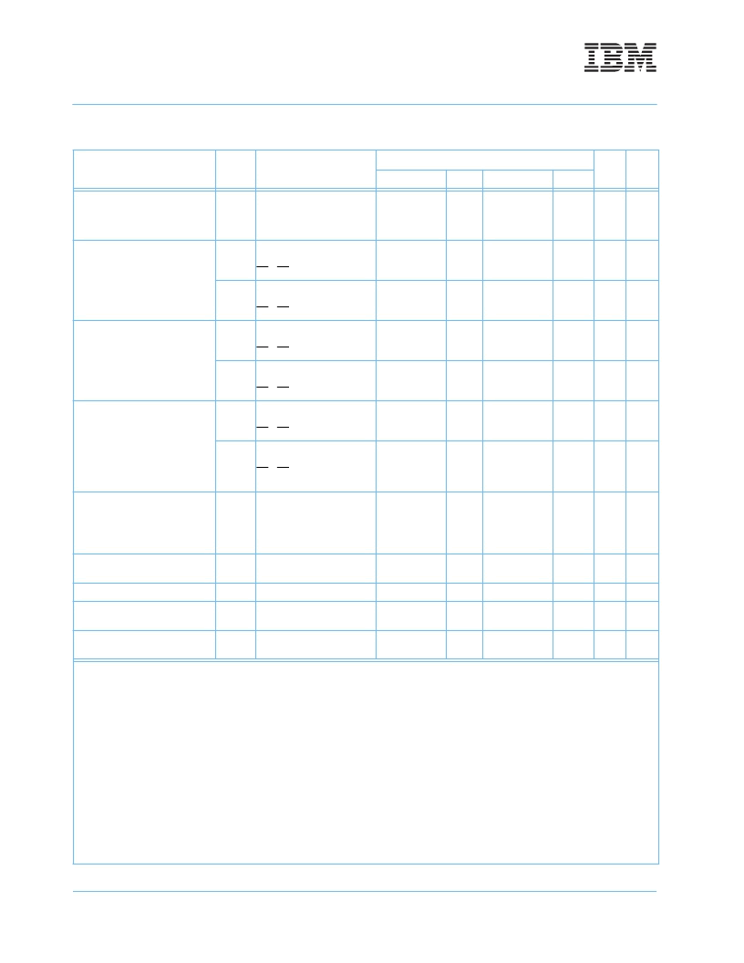
Operating, Standby, and Refresh Currents
(T
A
= 0 to +70
°
C, V
DD
= 3.3V
±
0.3V)
Parameter
Symbol
Test Condition
Speed/Organization
Units
Notes
-260, -360/x64 -10/x64 -260, -360/x72 -10/x72
Operating Current
t
=
t
(min), t
= min
Active-Precharge command
cycling without Burst operation
I
CC1
1 bank operation
920
680
1035
765
mA
1, 3, 4
Precharge Standby Current in
Power Down Mode
I
CC2P
CKE0, CKE1
≤
V
IL
(max),
t
= min,
S0 - S3 =V
IH
(min)
CKE0, CKE1
≤
V
IL
(max),
t
= Infinity,
S0 - S3 =V
IH
(min)
CKE0, CKE1
≥
V
IH
(min),
t
= min,
S0 - S3 =V
IH
(min)
CKE0, CKE1
≥
V
IH
(min),
t
= Infinity,
S0 - S3 =V
IH
(min)
CKE0, CKE1
≥
V
IH
(min),
t
= min,
S0 - S3 =V
IH
(min)
CKE0, CKE1
≤
V
IL
(max),
t
= min,
S0 - S3 =V
(min)
(Power Down Mode)
16
16
18
18
mA
2
I
CC2PS
16
16
18
18
mA
2
Precharge Standby Current in
Non-Power Down Mode
I
CC2N
400
400
450
450
mA
2, 5
I
CC2NS
96
96
108
108
mA
2, 6
No Operating Current
(Active state: 4 bank)
I
CC3N
640
480
720
540
mA
2, 5
I
CC3P
112
112
126
126
mA
2, 7
Burst Operating Current
I
CC4
t
= min,
Read/ Write command
cycling,
multiple banks active,
gapless data, BL = 4
960
960
1080
1080
mA
1, 4, 8
Auto (CBR) Refresh Current
I
CC5
t
= min,
CBR command cycling
1360
1120
1530
1260
mA
1
Self Refresh Current
I
CC6
CKE0, CKE1
≤
0.2V
16
16
18
18
mA
2
Serial PD Device Standby Cur-
rent
I
SB
V
IN
= GND or V
DD
30
30
30
30
μ
A
9
Serial PD Device Active Power
Supply Current
I
CCA
SCL Clock Frequency =
100KHz
1
1
1
1
mA
10
1. The specified values are for one DIMM bank in the specified mode, and the other DIMM bank in Active Standby (I
CC3N
).
2. The specified values are for both DIMM banks operating in the specified mode.
3. These parameters depend on the cycle rate and are measured with the cycle determined by the minimum value of t
CK
and t
RC
.
Input signals are changed up to three times during t
RC
(min).
4. The specified values are obtained with the output open.
5. Input signals are changed once during three clock cycles.
6. Input signals are stable.
7. Active Standby current will be higher if clock suspend is entered during a Burst Read cycle (add 1mA per DQ).
8. Input signals are changed once during t
CK(min)
.
9. V
DD
= 3.3V.
10. As follows:
Input pulse levels V
DD
x 0.1 to V
DD
x 0.9
Input rise and fall times 10ns
Input and output timing levels V
DD
x 0.5
Output load 1 TTL gate and CL=100pf
相關(guān)PDF資料 |
PDF描述 |
|---|---|
| IBMB3N16734HCB-260 | x72 SDRAM Module |
| IBMB3N16734HCB-360 | x72 SDRAM Module |
| IBMB3N16734HCB-75AT | x72 SDRAM Module |
| IBMB3N8644HCB-75AT | x64 SDRAM Module |
| IBMB3N8734HCB-75AT | x72 SDRAM Module |
相關(guān)代理商/技術(shù)參數(shù) |
參數(shù)描述 |
|---|---|
| IBMFDM44H-064J | 制造商:STEC Inc 功能描述:64MB FLASH 44PIN HORIZ IBM - Bulk |
| IBMFDM44H-064J-01 | 制造商:STEC Inc 功能描述:AKA:IBM00-01234-0A1C - Bulk |
| IBMFDM44H-064JU-01 | 制造商:STEC Inc 功能描述:AKA: IBM00-01234-0B1CU - Bulk |
| IBMFDM44H-128MM1U | 制造商:STEC Inc 功能描述:128MB CF, COMMERCIAL TEMP - Bulk |
| IBMN364164CT3C360 | 制造商:IBM 功能描述:* |
發(fā)布緊急采購,3分鐘左右您將得到回復(fù)。