- 您現(xiàn)在的位置:買賣IC網(wǎng) > PDF目錄360743 > ICS1572 GT 7C 7#16S SKT RECP WALL RM PDF資料下載
參數(shù)資料
| 型號(hào): | ICS1572 |
| 英文描述: | GT 7C 7#16S SKT RECP WALL RM |
| 中文描述: | 用戶可編程的差分輸出圖形時(shí)鐘發(fā)生器 |
| 文件頁(yè)數(shù): | 5/19頁(yè) |
| 文件大小: | 276K |
| 代理商: | ICS1572 |
第1頁(yè)第2頁(yè)第3頁(yè)第4頁(yè)當(dāng)前第5頁(yè)第6頁(yè)第7頁(yè)第8頁(yè)第9頁(yè)第10頁(yè)第11頁(yè)第12頁(yè)第13頁(yè)第14頁(yè)第15頁(yè)第16頁(yè)第17頁(yè)第18頁(yè)第19頁(yè)
Power-On Initialization
The
ICS1572
has an internal power-on reset circuit that per-
forms the following functions:
1)
Sets the multiplexer to pass the reference frequency
to the CLK+ and CLK- outputs.
2)
Selects the modulus of the N1 divider (for the
LOAD clock) to be four.
These functions should allow initialization of most graphics
systems that cannot immediately provide for register program-
ming upon system power-up.
Because the power-on reset circuit is on the VDD supply, and
because that supply is filtered, care must be taken to allow the
reset to de-assert before programming. A safe guideline is to
allow 20 microseconds after the VDD supply reaches 4 volts.
Programming Notes
VCO Frequency Range: Use the post-divider to keep the
VCO frequency as high as possible within its operating
range.
Divider Range: For best results in normal situations (i.e.,
pixel clock generation for hi-res displays), keep the refer-
ence divider modulus as short as possible (for a frequency
at the output of the reference divider in the few hundred
kHz to several MHz range). If you need to go to a lower
phase comparator reference frequency (usually required
for increased frequency accuracy), that is acceptable, but
jitter performance will suffer somewhat.
VCO Gain Programming: Use the minimum gain which
can reliably achieve the VCO frequency desired, as shown
here:
VCO GAIN
4
5
6
7
MAX FREQUENCY
120 MHz
200 MHz
230 MHz
*
* SPECIAL APPLICATION. Contact factory for custom product above
230 MHz.
Phase Detector Gain: For most graphics applications and
divider ranges, set P[1,0] = 10 and set P[2] = 1. Under
some circumstances, setting the P[2] bit “on” can reduce
jitter. During 1572 operation at exact multiples of the
crystal frequency, P[2] bit = 0 may provide the best jitter
performance.
Board Test Support
It is often desirable to statically control the levels of the output
pins for circuit board test. The
ICS1572
supports this through
a register programmable mode, AUXEN. When this mode is
set, two register bits directly control the logic levels of the
CLK+/CLK- pins and the LOAD pin. This mode is activated
when the S[0] and S[1] bits are both set to logic 1. See Register
Mapping for details.
Power Supplies and Decoupling
The
ICS1572
has two VSS pins to reduce the effects of package
inductance. Both pins are connected to the same potential on
the die (the ground bus). BOTH of these pins should connect
to the ground plane of the video board as close to the package
as is possible.
The
ICS1572
has a VDDO pin which is the supply of +5 volt
power to all output drivers. This pin should be connected to the
power plane (or bus) using standard high-frequency decou-
pling practice. That is, capacitors should have low series induc-
tance and be mounted close to the
ICS1572
.
The VDD pin is the power supply pin for the PLL synthesizer
circuitry and other lower current digital functions. We recom-
mend that RC decoupling or zener regulation be provided for
this pin (as shown in the recommended application circuitry).
This will allow the PLL to “track” through power supply
fluctuations without visible effects. See Figure 7 for typical
external circuitry.
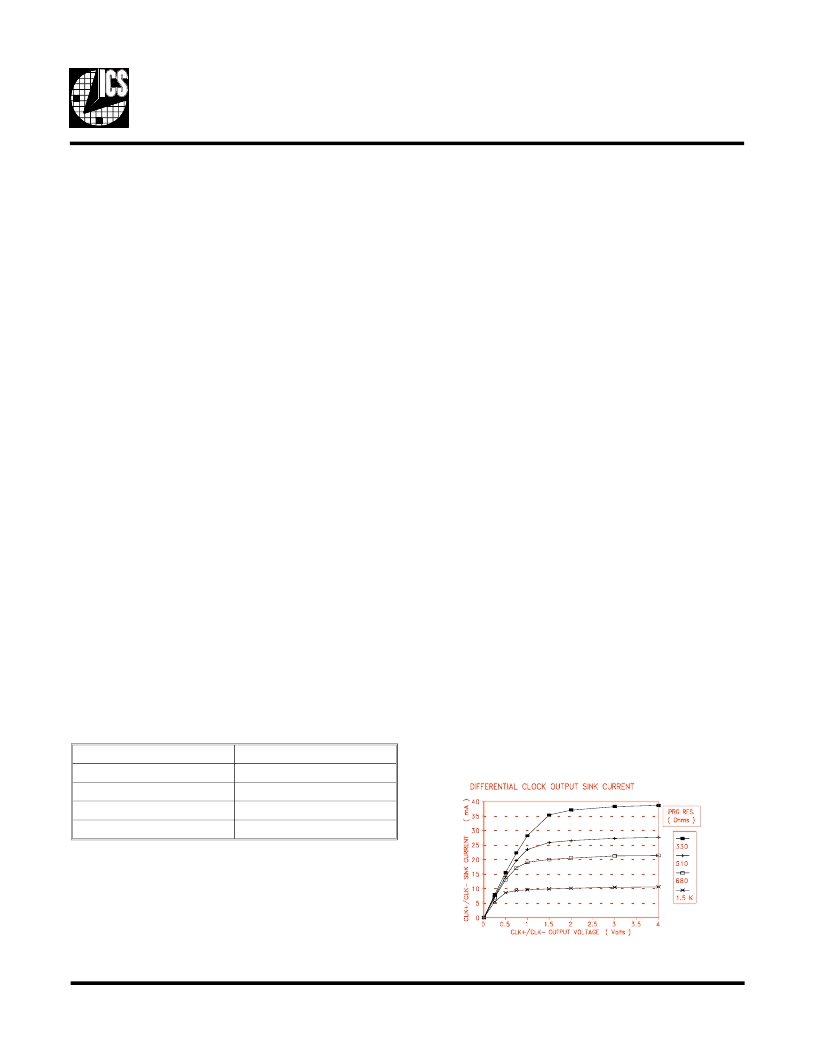
Figure 6
ICS1572
5
相關(guān)PDF資料 |
PDF描述 |
|---|---|
| ICS1572M-101 | GT 4C 4#12 PIN RECP WALL RM |
| ICS1572M-301 | GT 4C 4#12 SKT RECP WALL RM |
| ICS1574B | GT 5C 5#12 PIN RECP WALL RM |
| ICS1574BEB | GT 5C 5#12 SKT RECP WALL RM |
| ICS1574BM | GT 10C 10#16 PIN RECP WALL RM |
相關(guān)代理商/技術(shù)參數(shù) |
參數(shù)描述 |
|---|---|
| ICS1572M101 | 制造商:未知廠家 制造商全稱:未知廠家 功能描述:Video/Graphics Clock Generator |
| ICS1572M-101 | 制造商:ICS 制造商全稱:ICS 功能描述:User Programmable Differential Output Graphics Clock Generator |
| ICS1572M301 | 制造商:未知廠家 制造商全稱:未知廠家 功能描述:Video/Graphics Clock Generator |
| ICS1572M-301 | 制造商:ICS 制造商全稱:ICS 功能描述:User Programmable Differential Output Graphics Clock Generator |
| ICS1574B | 制造商:ICS 制造商全稱:ICS 功能描述:User Programmable Laser Engine Pixel Clock Generator |
發(fā)布緊急采購(gòu),3分鐘左右您將得到回復(fù)。