- 您現(xiàn)在的位置:買賣IC網(wǎng) > PDF目錄67685 > ICS5342 PALETTE-DAC DSPL CTLR, PQCC68 PDF資料下載
參數(shù)資料
| 型號(hào): | ICS5342 |
| 元件分類: | 顯示控制器 |
| 英文描述: | PALETTE-DAC DSPL CTLR, PQCC68 |
| 封裝: | PLASTIC, LCC-68 |
| 文件頁數(shù): | 31/36頁 |
| 文件大小: | 1017K |
| 代理商: | ICS5342 |
第1頁第2頁第3頁第4頁第5頁第6頁第7頁第8頁第9頁第10頁第11頁第12頁第13頁第14頁第15頁第16頁第17頁第18頁第19頁第20頁第21頁第22頁第23頁第24頁第25頁第26頁第27頁第28頁第29頁第30頁當(dāng)前第31頁第32頁第33頁第34頁第35頁第36頁
ICS5342
GENDAC
4
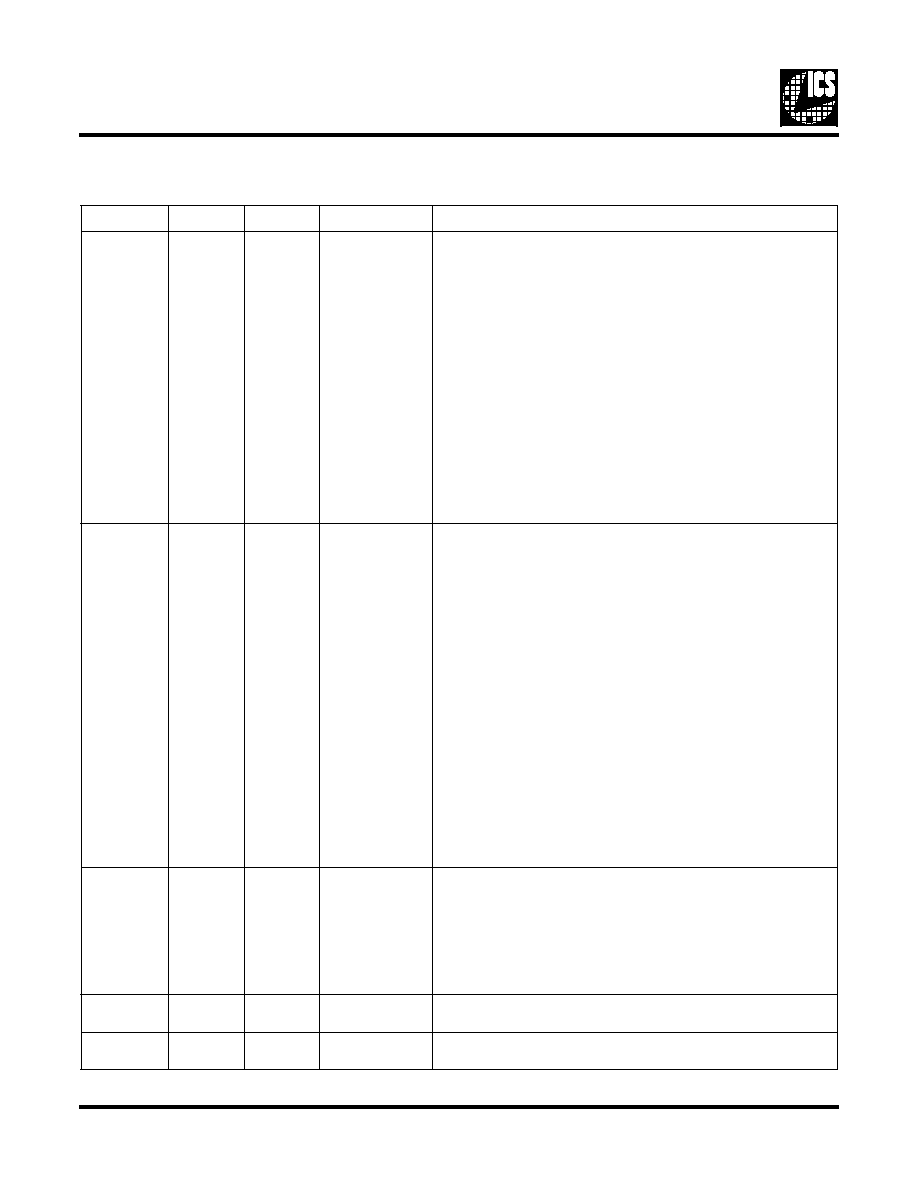
Internal Registers
RS2
RS1
RS0
Register Name
Description (all registers can be written to and read from)
The GENDAC has a single pixel address register which can be
accessed through either register address 0,0,0 or 0,1,1 – reading
from either register gives the same result.
Writing a value to address 0,0,0:
– species an address within the color palette RAM
– initializes the Color Value register
Writing a value to address 0,1,1:
– species an address within the color palette RAM
– loads Color Value register with contents of location in
addressed RAM palette and then:
– increments Pixel Address register
0
1
Pixel Address
WRITE
Writing to this 8-bit register is done before writing one or more
color values to color palette RAM.
0
1
Pixel Address
READ
Writing to this 8-bit register is done before reading one or more
color values from color palette RAM.
0
1
Color Value
The 18-bit Color Value register acts as a buffer between the
microprocessor interface and the color palette. A value may be
read from or written to this register using a three-byte transfer
sequence. The color value is contained in the least signicant 6
bits, D0-D5, of the byte read – the most signicant 2 bits are set
to zero. The same 6 bits are used when writing a byte. When
reading or writing, data is transferred in the same order – red
byte rst, then green, then blue. Each transfer between the Color
Value register and the color palette replaces the normal pixel
mapping operations of the GENDAC for a single pixel.
After writing three denitions to this register, its contents are
written to the location in the color palette RAM specied by the
Pixel Address register, before that register increments.
After reading three denitions from this register, the contents of
the location in the color palette RAM specied by the Pixel
Address registers are copied into the Color Value register, and
the Pixel Address register increments.
0
1
0
Pixel Mask
The 8-bit Pixel Mask register can be used to mask selected bits
of the Pixel Address value applied to the Pixel Address inputs
(P7-P0). A one in a position in the mask register leaves the corre-
sponding bit in the Pixel Address unaltered, while a zero sets
that bit to zero. The Pixel Mask register does not affect the Pixel
Address generated by the microprocessor interface when the pal-
ette RAM is being accessed.
1
0
PLL Address
WRITE
Writing to this 8-bit register is performed prior to writing one or
more PLL programming values to the PLL Parameter register.
1
PLL Address
READ
Writing to this 8-bit register is performed prior to reading one or
more PLL programming values from the PLL Parameter register.
相關(guān)PDF資料 |
PDF描述 |
|---|---|
| ICS552ARI-01LFT | 200 MHz, OTHER CLOCK GENERATOR, PDSO20 |
| ICS552R-01ILF | 200 MHz, OTHER CLOCK GENERATOR, PDSO20 |
| ICS557G-05ATR | 200 MHz, PROC SPECIFIC CLOCK GENERATOR, PDSO20 |
| ICS557G-08LF | 557 SERIES, LOW SKEW CLOCK DRIVER, 1 TRUE OUTPUT(S), 0 INVERTED OUTPUT(S), PDSO16 |
| ICS557G-08LFT | 557 SERIES, LOW SKEW CLOCK DRIVER, 1 TRUE OUTPUT(S), 0 INVERTED OUTPUT(S), PDSO16 |
相關(guān)代理商/技術(shù)參數(shù) |
參數(shù)描述 |
|---|---|
| ICS5342-1 | 制造商:ICS 制造商全稱:ICS 功能描述:Analog IC |
| ICS5342-2 | 制造商:ICS 制造商全稱:ICS 功能描述:Analog IC |
| ICS5342-3 | 制造商:ICS 制造商全稱:ICS 功能描述:Analog IC |
| ICS5342ADD | 制造商:ICS 制造商全稱:ICS 功能描述:Addendum to ICS5342 Data Sheet |
| ICS5342V | 制造商:未知廠家 制造商全稱:未知廠家 功能描述:Peripheral IC |
發(fā)布緊急采購,3分鐘左右您將得到回復(fù)。