- 您現(xiàn)在的位置:買賣IC網(wǎng) > PDF目錄377480 > IDT54FCT388915T133PYB (INTEGRATED DEVICE TECHNOLOGY INC) 3.3V LOW SKEW PLL-BASED CMOS CLOCK DRIVER WITH (3-STATE) PDF資料下載
參數(shù)資料
| 型號: | IDT54FCT388915T133PYB |
| 廠商: | INTEGRATED DEVICE TECHNOLOGY INC |
| 元件分類: | 時鐘及定時 |
| 英文描述: | 3.3V LOW SKEW PLL-BASED CMOS CLOCK DRIVER WITH (3-STATE) |
| 中文描述: | FCT SERIES, PLL BASED CLOCK DRIVER, 7 TRUE OUTPUT(S), 1 INVERTED OUTPUT(S), PDSO28 |
| 封裝: | 5.30 MM, 0.65 MM PITCH, SSOP-28 |
| 文件頁數(shù): | 1/11頁 |
| 文件大小: | 145K |
| 代理商: | IDT54FCT388915T133PYB |
IDT54/74FCT388915T 70/100/133/150
3.3V LOW SKEW PLL-BASED CLOCK DRIVER
MILITARY AND COMMERCIAL TEMPERATURE RANGES
IDT54/74FCT388915T
9.8
Integrated Device Technology, Inc.
The IDT logo is a registered trademark of Integrated Device Technology, Inc.
MILITARY AND COMMERCIAL TEMPERATURE RANGES
FEATURES:
0.5 MICRON CMOS Technology
Input frequency range: 10MHz – f2Q Max. spec
(FREQ_SEL = HIGH)
Max. output frequency: 150MHz
Pin and function compatible with FCT88915T, MC88915T
5 non-inverting outputs, one inverting output, one 2x
output, one
÷
2 output; all outputs are TTL-compatible
3-State outputs
Output skew < 350ps (max.)
Duty cycle distortion < 500ps (max.)
Part-to-part skew: 1ns (from t
PD
max. spec)
32/–16mA drive at CMOS output voltage levels
V
CC
= 3.3V
±
0.3V
Inputs can be driven by 3.3V or 5V components
Available in 28 pin PLCC, LCC and SSOP packages
DESCRIPTION:
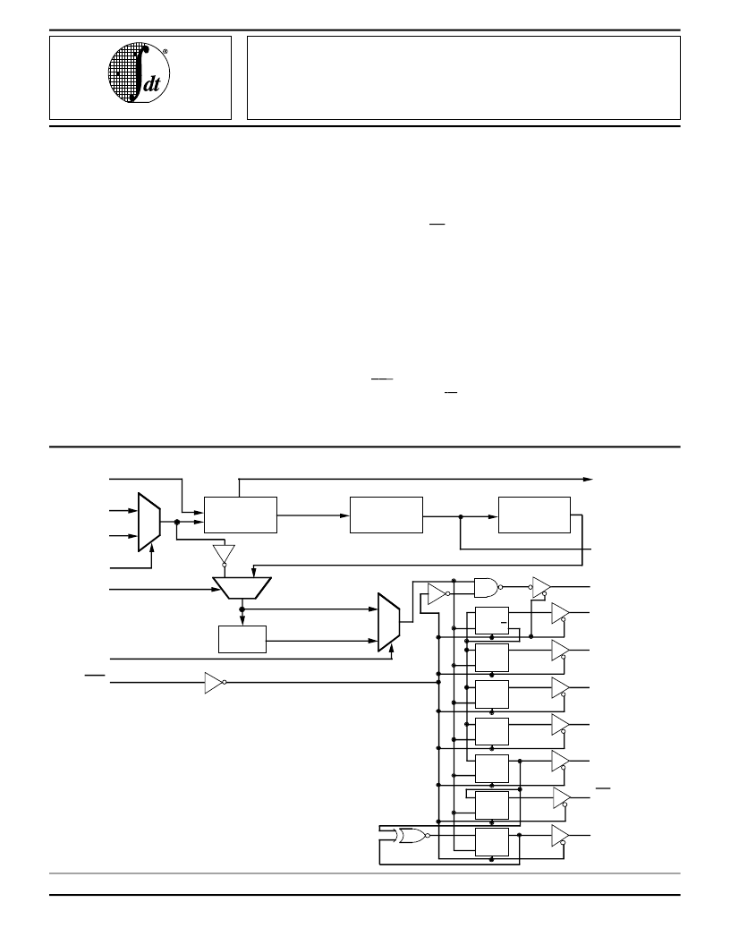
The IDT54/74FCT388915T uses phase-lock loop technol-
ogy to lock the frequency and phase of outputs to the input
reference clock. It provides low skew clock distribution for
high performance PCs and workstations. One of the outputs
FUNCTIONAL BLOCK DIAGRAM
1
AUGUST 1995
1995 Integrated Device Technology, Inc.
9.8
DSC-4243/1
is fed back to the PLL at the FEEDBACK input resulting in
essentially zero delay across the device. The PLL consists of
the phase/frequency detector, charge pump, loop filter and
VCO. The VCO is designed for a 2Q operating frequency
range of 40MHz to f2Q Max.
The IDT54/74FCT388915T provides 8 outputs with 350ps
skew. The
Q5
output is inverted from the Q outputs. The 2Q
runs at twice the Q frequency and Q/2 runs at half the Q
frequency.
The FREQ_SEL control provides an additional
÷
2 option in
the output path. PLL _EN allows bypassing of the PLL, which
is useful in static test modes. When PLL_EN is low, SYNC
input may be used as a test clock. In this test mode, the input
frequency is not limited to the specified range and the polarity
of outputs is complementary to that in normal operation
(PLL_EN = 1). The LOCK output attains logic HIGH when the
PLL is in steady-state phase and frequency lock. When OE/
RST
is low, all the outputs are put in high impedance state and
registers at Q,
Q
and Q/2 outputs are reset.
The IDT54/74FCT388915T requires one external loop filter
component as recommended in Figure 3.
70/100/133/150
PRELIMINARY
3.3V LOW SKEW PLL-BASED
CMOS CLOCK DRIVER
(WITH 3-STATE)
Phase/Freq.
Detector
M
u
x
0
1
SYNC (0)
FEEDBACK
SYNC (1)
REF_SEL
PLL_EN
Mux
0
1
Divide
-By-2
(
÷
1)
(
÷
2)
1
0
M
u
x
Charge Pump
Voltage
Controlled
Oscilator
OE/RST
FREQ_SEL
2Q
Q0
Q1
Q2
Q3
Q4
Q5
Q/2
D
Q
CP
Q
R
R
D
Q
CP
R
D
Q
CP
R
D
Q
CP
R
D
Q
CP
R
D
Q
CP
R
D
Q
CP
LF
LOCK
3052 drw 01
相關(guān)PDF資料 |
PDF描述 |
|---|---|
| IDT74FCT388915T133PYB | 3.3V LOW SKEW PLL-BASED CMOS CLOCK DRIVER WITH (3-STATE) |
| IDT74FCT388915T70 | 3.3V LOW SKEW PLL-BASED CMOS CLOCK DRIVER WITH (3-STATE) |
| IDT54FCT388915T70 | 3.3V LOW SKEW PLL-BASED CMOS CLOCK DRIVER WITH (3-STATE) |
| IDT54FCT388915T70J | 3.3V LOW SKEW PLL-BASED CMOS CLOCK DRIVER WITH (3-STATE) |
| IDT74FCT388915T70J | 3.3V LOW SKEW PLL-BASED CMOS CLOCK DRIVER WITH (3-STATE) |
相關(guān)代理商/技術(shù)參數(shù) |
參數(shù)描述 |
|---|---|
| IDT54FCT521ADB | 制造商:Integrated Device Technology Inc 功能描述: |
| IDT54FCT533DB | 制造商:Integrated Device Technology Inc 功能描述: |
| IDT54FCT543ADB | 制造商:MAJOR 功能描述: |
| IDT54FCT543ATDB | 制造商:MAJOR 功能描述: |
| IDT54FCT573ADB | 制造商:Integrated Device Technology Inc 功能描述: |
發(fā)布緊急采購,3分鐘左右您將得到回復(fù)。