- 您現(xiàn)在的位置:買賣IC網(wǎng) > PDF目錄377403 > IDT72201L15PFI (INTEGRATED DEVICE TECHNOLOGY INC) SerDes Low Voltage 24-Bit Bi-Directional Serializer/Deserializer; Package: MLP; No of Pins: 40; Container: Tape & Reel PDF資料下載
參數(shù)資料
| 型號(hào): | IDT72201L15PFI |
| 廠商: | INTEGRATED DEVICE TECHNOLOGY INC |
| 元件分類: | DRAM |
| 英文描述: | SerDes Low Voltage 24-Bit Bi-Directional Serializer/Deserializer; Package: MLP; No of Pins: 40; Container: Tape & Reel |
| 中文描述: | 256 X 9 OTHER FIFO, 10 ns, PQFP32 |
| 封裝: | TQFP-32 |
| 文件頁(yè)數(shù): | 2/14頁(yè) |
| 文件大?。?/td> | 155K |
| 代理商: | IDT72201L15PFI |
第1頁(yè)當(dāng)前第2頁(yè)第3頁(yè)第4頁(yè)第5頁(yè)第6頁(yè)第7頁(yè)第8頁(yè)第9頁(yè)第10頁(yè)第11頁(yè)第12頁(yè)第13頁(yè)第14頁(yè)
COMMERCIAL AND INDUSTRIAL
TEMPERATURE RANGES
IDT72421/72201/72211/72221/72231/72241/72251 CMOS SyncFIFO
64 x 9, 256 x 9, 512 x 9, 1,024 x 9, 2,048 x 9, 4,096 x 9 and 8,192 x 9
2
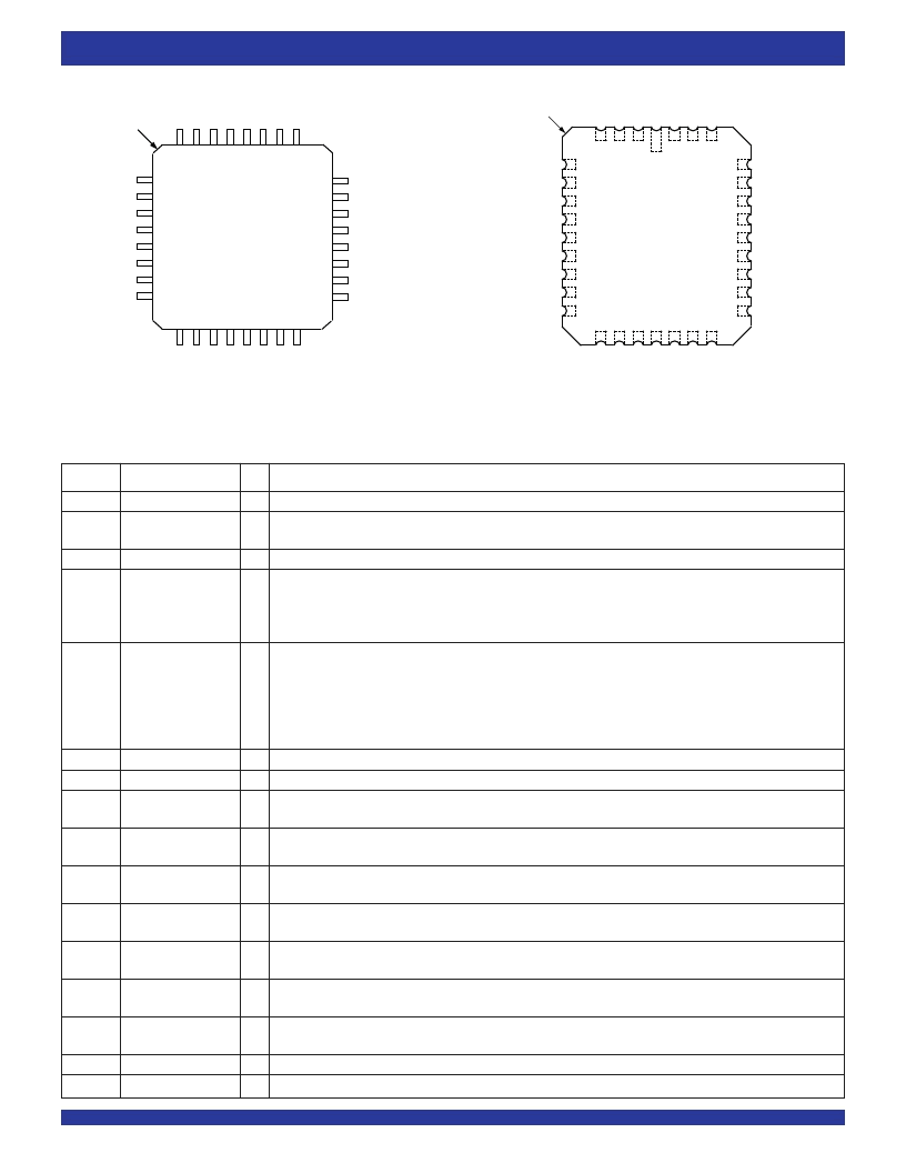
PIN CONFIGURATION
TQFP (PR32-1, order code: PF)
TOP VIEW
PLCC (J32-1, order code: J)
TOP VIEW
R
WEN1
WCLK
WEN2/
LD
V
CC
Q
8
Q
7
5
6
7
8
16
D
0
PAF
PAE
GND
REN1
RCLK
REN2
27 26 25
24
23
22
21
20
19
29 28
32 31 30
9 10 11 12 13 14 15
2655 drw 02
E
O
F
1
2
3
4
18
17
INDEX
D
1
Q
0
Q
1
Q
2
Q
3
Q
4
Q
6
Q
5
D
2
D
3
D
4
D
5
D
6
D
7
D
8
RS
WEN1
WCLK
WEN2/
LD
V
CC
Q
8
5
6
7
8
9
10
11
12
13
PAF
PAE
GND
REN1
RCLK
REN2
OE
27
26
25
24
23
22
21
29
28
4
3
2
1
32 31 30
14 15 16 17 18 19 20
D
2
F
E
INDEX
2655 drw02a
D
3
D
4
D
5
D
6
D
7
D
8
Q
0
Q
1
Q
2
Q
3
Q
4
Q
7
Q
6
Q
5
D
1
D
0
Symbol
D
0
-D
8
RS
Name
I/O
I
I
Description
Data Inputs
Reset
Data inputs for a 9-bit bus.
When
RS
is set LOW, internal read and write pointers are set to the first location of the RAM array,
FF
and
PAF
go HIGH, and
PAE
and
EF
go LOW. A reset is required before an initial WRITE after power-up.
Data is written into the FIFO on a LOW-to-HIGH transition of WCLK when the Write Enable(s) are asserted.
If the FIFO is configured to have programmable flags,
WEN1
is the only write enable pin. When
WEN1
is LOW,
data is written into the FIFO on every LOW-to-HIGH transition WCLK. If the FIFO is configured to have two write
enables,
WEN1
must be LOW and WEN2 must be HIGH to write data into the FIFO. Data will not be written into
the FIFO if the
FF
is LOW.
The FIFO is configured at reset to have either two write enables or programmable flags. If WEN2/
LD
is
HIGH
at reset, this pin operates as a second write enable. If WEN2/
LD
is LOW at reset, this pin operates as a control
to load and read the programmable flag offsets. If the FIFO is configured to have two write enables,
WEN1
must
be LOW and WEN2 must be HIGH to write data into the FIFO. Data will not be written into the FIFO if the
FF
is
LOW. If the FIFO is configured to have programmable flags, WEN2/
LD
is held LOW to write or read the
programmable flag offsets.
O Data outputs for a 9-bit bus.
I
Data is read fromthe FIFO on a LOW-to-HIGH transition of RCLK when
REN1
and
REN2
are asserted.
I
When
REN1
and
REN2
are LOW, data is read fromthe FIFO on every LOW-to-HIGH transition of RCLK.
Data will not be read fromthe FIFO if the
EF
is LOW.
I
When
REN1
and
REN2
are LOW, data is read fromthe FIFO on every LOW-to-HIGH transition of RCLK.
Data will not be read fromthe FIFO if the
EF
is LOW.
I
When
OE
is LOW, the data output bus is active. If
OE
is HIGH, the output data bus will be in a high-impedance
state.
O When
EF
is LOW, the FIFO is empty and further data reads fromthe output are inhibited. When
EF
is HIGH, the
FIFO is not empty.
EF
is synchronized to RCLK.
O When
PAE
is LOW, the FIFO is almost-empty based on the offset programmed into the FIFO. The default
offset at reset is Empty+7.
PAE
is synchronized to RCLK.
O When
PAF
is LOW, the FIFO is almost-full based on the offset programmed into the FIFO. The default offset
at reset is Full-7.
PAF
is synchronized to WCLK.
O When
FF
is LOW, the FIFO is full and further data writes into the input are inhibited. When
FF
is HIGH, the FIFO
is not full.
FF
is synchronized to WCLK.
One +5 volt power supply pin.
One 0 volt ground pin.
WCLK
WEN1
Write Clock
Write Enable 1
I
I
WEN2/
LD
Write Enable 2/
Load
I
Q
0
-Q
8
RCLK
REN1
Data Outputs
Read Clock
Read Enable 1
REN2
Read Enable 2
OE
Output Enable
EF
Empty Flag
PAE
Programmable
Almost-Empty Flag
Programmable
Almost-Full Flag
Full Flag
PAF
FF
V
CC
GND
Power
Ground
PIN DESCRIPTIONS
相關(guān)PDF資料 |
PDF描述 |
|---|---|
| IDT72201L25J | 24-Bit Ultra-Low Power Serializer Deserializer Supporting Single and Dual Displays (*Recommended for new designs); Package: BGA; No of Pins: 42; Container: Tape & Reel |
| IDT72201L25JI | 24-Bit Ultra-Low Power Serializer Deserializer Supporting Single and Dual Displays (*Recommended for new designs); Package: MLP; No of Pins: 40; Container: Tape & Reel |
| IDT72201L25PF | Low Voltage 28-Bit Flat Panel Display Link Serializers |
| IDT72201L25PFI | Low Voltage 28-Bit Flat Panel Display Link Serializers; Package: TSSOP; No of Pins: 56; Container: Tape & Reel |
| IDT72251L10J | CMOS SyncFIFOO 64 X 9, 256 x 9, 512 x 9, 1024 X 9, 2048 X 9 and 4096 x 9 |
相關(guān)代理商/技術(shù)參數(shù) |
參數(shù)描述 |
|---|---|
| IDT72201L15PFI8 | 功能描述:IC FIFO 256X9 SYNC 15NS 32-TQFP RoHS:否 類別:集成電路 (IC) >> 邏輯 - FIFO 系列:7200 標(biāo)準(zhǔn)包裝:80 系列:7200 功能:同步 存儲(chǔ)容量:18.4K(1K x 18) 數(shù)據(jù)速率:- 訪問時(shí)間:10ns 電源電壓:4.5 V ~ 5.5 V 工作溫度:0°C ~ 70°C 安裝類型:表面貼裝 封裝/外殼:64-LQFP 供應(yīng)商設(shè)備封裝:64-TQFP(10x10) 包裝:托盤 其它名稱:72225LB10TF |
| IDT72201L20J | 制造商:Integrated Device Technology Inc 功能描述:FIFO, 256 x 9, Synchronous, 32 Pin, Plastic, PLCC |
| IDT72201L25J | 功能描述:IC FIFO 256X9 SYNC 25NS 32-PLCC RoHS:否 類別:集成電路 (IC) >> 邏輯 - FIFO 系列:7200 標(biāo)準(zhǔn)包裝:90 系列:74ABT 功能:同步,雙端口 存儲(chǔ)容量:4.6K(64 x 36 x2) 數(shù)據(jù)速率:67MHz 訪問時(shí)間:- 電源電壓:4.5 V ~ 5.5 V 工作溫度:0°C ~ 70°C 安裝類型:表面貼裝 封裝/外殼:120-LQFP 裸露焊盤 供應(yīng)商設(shè)備封裝:120-HLQFP(14x14) 包裝:托盤 產(chǎn)品目錄頁(yè)面:1005 (CN2011-ZH PDF) 其它名稱:296-3984 |
| IDT72201L25J8 | 功能描述:IC FIFO 256X9 SYNC 25NS 32-PLCC RoHS:否 類別:集成電路 (IC) >> 邏輯 - FIFO 系列:7200 標(biāo)準(zhǔn)包裝:80 系列:7200 功能:同步 存儲(chǔ)容量:18.4K(1K x 18) 數(shù)據(jù)速率:- 訪問時(shí)間:10ns 電源電壓:4.5 V ~ 5.5 V 工作溫度:0°C ~ 70°C 安裝類型:表面貼裝 封裝/外殼:64-LQFP 供應(yīng)商設(shè)備封裝:64-TQFP(10x10) 包裝:托盤 其它名稱:72225LB10TF |
| IDT72201L25JI | 功能描述:IC FIFO 256X9 SYNC 25NS 32-PLCC RoHS:否 類別:集成電路 (IC) >> 邏輯 - FIFO 系列:7200 標(biāo)準(zhǔn)包裝:80 系列:7200 功能:同步 存儲(chǔ)容量:18.4K(1K x 18) 數(shù)據(jù)速率:- 訪問時(shí)間:10ns 電源電壓:4.5 V ~ 5.5 V 工作溫度:0°C ~ 70°C 安裝類型:表面貼裝 封裝/外殼:64-LQFP 供應(yīng)商設(shè)備封裝:64-TQFP(10x10) 包裝:托盤 其它名稱:72225LB10TF |
發(fā)布緊急采購(gòu),3分鐘左右您將得到回復(fù)。