- 您現(xiàn)在的位置:買(mǎi)賣(mài)IC網(wǎng) > PDF目錄224008 > IDT74FST3126Q8 (INTEGRATED DEVICE TECHNOLOGY INC) CBT/FST/QS/5C/B SERIES, 4-BIT DRIVER, TRUE OUTPUT, PDSO16 PDF資料下載
參數(shù)資料
| 型號(hào): | IDT74FST3126Q8 |
| 廠商: | INTEGRATED DEVICE TECHNOLOGY INC |
| 元件分類: | 總線收發(fā)器 |
| 英文描述: | CBT/FST/QS/5C/B SERIES, 4-BIT DRIVER, TRUE OUTPUT, PDSO16 |
| 封裝: | QSOP-16 |
| 文件頁(yè)數(shù): | 3/5頁(yè) |
| 文件大小: | 77K |
| 代理商: | IDT74FST3126Q8 |
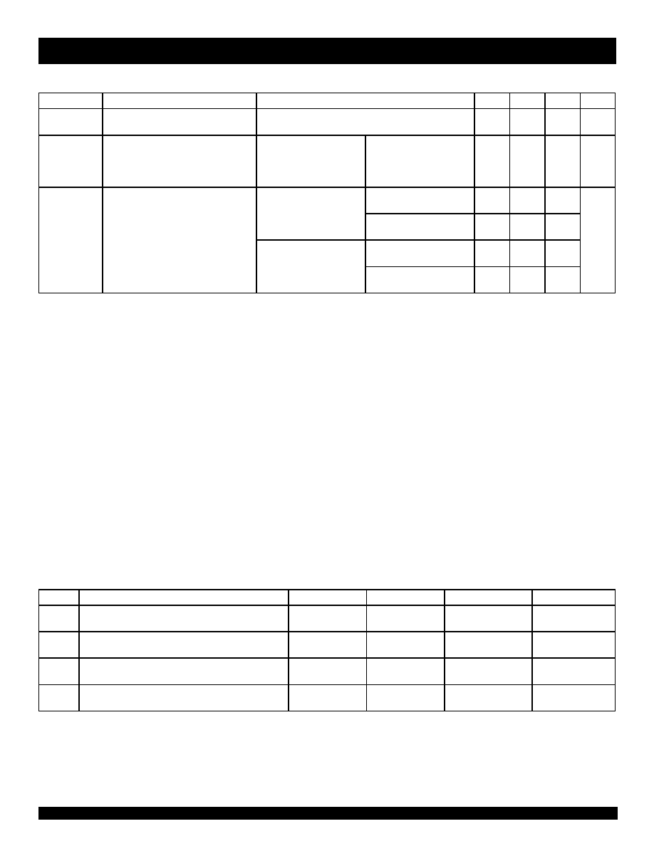
3
IDT74FST3126
QUADRUPLE BUS SWITCH WITH INDIVIDUAL POSITIVE ENABLES
COMMERCIALTEMPERATURERANGE
POWER SUPPLY CHARACTERISTICS
Symbol
Parameter
Test Conditions(1)
Min.
Typ.(2)
Max.
Unit
ICC
Quiescent Power Supply Current
TTL Inputs HIGH
VCC = Max.
VIN = 3.4V(3)
—0.5
1.5
mA
ICCD
Dynamic Power Supply Current(4,5)
VCC = Max.
Outputs Open
VIN = VCC
VIN = GND
—35
55
A/
MHz/
One Enable Pin Toggling
50% Duty Cycle
Enable
IC
Total Power Supply Current(6)
VCC = Max.
One Enable Pin Toggling
VIN = VCC
VIN = GND
—
0.35
0.55
mA
fi = 10MHz
50% Duty Cycle
VIN = 3.4
VIN = GND
0.6
1.3
VCC = Max.
4 Enable Pins Toggling
VIN = VCC
VIN = GND
1.4
2.2
fi = 10MHz
50% Duty Cycle
VIN = 3.4
VIN = GND
—2.4
5.2
NOTES:
1. For conditions shown as Max. or Min., use appropriate value specified under Electrical Characteristics for the applicable device type. TA = –40°C to
+85°C
2. Typical values are at VCC = 5.0V, +25°C ambient.
3. Per TTL driven input (VIN = 3.4V). All other inputs at VCC or GND. Switch inputs do not contribute to
ICC.
4. This parameter represents the current required to switch the internal capacitance of the control inputs at the specified frequency.
Switch inputs generate no significant power supply currents as they transition. This parameter is not directly testable, but is derived for use in Total
Power Supply Calculations.
5. CPD = ICCD/VCC
CPD = Power Dissipation Capacitance
6. IC = IQUIESCENT + IINPUTS + IDYNAMIC
IC = ICC +
ICC DHNT + ICCD (fiN)
ICC = Quiescent Current
ICC = Power Supply Current for a TTL High Input (VIN = 3.4V)
DH = Duty Cycle for TTL Inputs High
NT = Number of TTL Inputs at DH
ICCD = Dynamic Current Caused by an Input Transition Pair (HLH or LHL)
fi = Control Input Frequency
N = Number of Control Inputs Toggling at fi
SWITCHING CHARACTERISTICS OVER OPERATING RANGE
Following Conditions Apply Unless Otherwise Specified:
Commercial: TA = -40°C to +85°C, VCC = 5.0V ± 10%
Symbol
Description
Min.(2)
Typ.
Max.
Unit
tPLH
tPHL
Data Propagation Delay
xA to xB(2)
—
0.25
ns
tPZH
tPZL
Switch CONNECT Delay
OE to xA, xB
1.5
—
6.5
ns
tPHZ
tPLZ
Switch DISCONNECT Delay
OE to xA, xB
1.5
—
5.5
ns
|QCI|
Charge Injection, During Switch DISCONNECT,
xOE to A or B(3)
—1.5
—
pC
NOTES:
1. See test circuits and waveforms.
2. The bus switch contributes no Propagation Delay other than the RC Delay of the load interacting with the RC of the switch.
3. |QCI| is the charge injection for a single switch DISCONNECT and applies to either single switches or multiplexers.
|QDCI| is the charge injection for a multiplexer as the multiplexed port switches from one path to another. Charge injection is reduced because the
injection from the DISCONNECT of the first path is compensated by the CONNECT of the second path.
相關(guān)PDF資料 |
PDF描述 |
|---|---|
| IDT74FST3383PG8 | CBT/FST/QS/5C/B SERIES, DUAL 4-BIT EXCHANGER, TRUE OUTPUT, PDSO24 |
| IDT74LVCH16244APAG8 | LVC/LCX/Z SERIES, QUAD 4-BIT DRIVER, TRUE OUTPUT, PDSO48 |
| IDT74SSTUAE32866ABFG8 | SSTU SERIES, POSITIVE EDGE TRIGGERED D FLIP-FLOP, TRUE OUTPUT, PBGA96 |
| IDTCV132BPVG | 200 MHz, PROC SPECIFIC CLOCK GENERATOR, PDSO56 |
| IDTCV174CPAG8 | 400 MHz, PROC SPECIFIC CLOCK GENERATOR, PDSO56 |
相關(guān)代理商/技術(shù)參數(shù) |
參數(shù)描述 |
|---|---|
| IDT74FST32383FPG | 制造商:Rochester Electronics LLC 功能描述:- Bulk |
| IDT74FST32384FSO | 制造商:Rochester Electronics LLC 功能描述:- Bulk 制造商:Integrated Device Technology Inc 功能描述: |
| IDT74FST3244FPG | 制造商:Integrated Device Technology Inc 功能描述: |
| IDT74FST3244FSO | 制造商:Rochester Electronics LLC 功能描述:- Bulk |
| IDT74FST3244PG | 制造商:Integrated Device Technology Inc 功能描述: |
發(fā)布緊急采購(gòu),3分鐘左右您將得到回復(fù)。