- 您現(xiàn)在的位置:買賣IC網(wǎng) > PDF目錄45382 > IR80C52EXXX-36:R (ATMEL CORP) 8-BIT, MROM, 36 MHz, MICROCONTROLLER, CQCC44 PDF資料下載
參數(shù)資料
| 型號(hào): | IR80C52EXXX-36:R |
| 廠商: | ATMEL CORP |
| 元件分類: | 微控制器/微處理器 |
| 英文描述: | 8-BIT, MROM, 36 MHz, MICROCONTROLLER, CQCC44 |
| 封裝: | LCC-44 |
| 文件頁數(shù): | 150/352頁 |
| 文件大小: | 7093K |
第1頁第2頁第3頁第4頁第5頁第6頁第7頁第8頁第9頁第10頁第11頁第12頁第13頁第14頁第15頁第16頁第17頁第18頁第19頁第20頁第21頁第22頁第23頁第24頁第25頁第26頁第27頁第28頁第29頁第30頁第31頁第32頁第33頁第34頁第35頁第36頁第37頁第38頁第39頁第40頁第41頁第42頁第43頁第44頁第45頁第46頁第47頁第48頁第49頁第50頁第51頁第52頁第53頁第54頁第55頁第56頁第57頁第58頁第59頁第60頁第61頁第62頁第63頁第64頁第65頁第66頁第67頁第68頁第69頁第70頁第71頁第72頁第73頁第74頁第75頁第76頁第77頁第78頁第79頁第80頁第81頁第82頁第83頁第84頁第85頁第86頁第87頁第88頁第89頁第90頁第91頁第92頁第93頁第94頁第95頁第96頁第97頁第98頁第99頁第100頁第101頁第102頁第103頁第104頁第105頁第106頁第107頁第108頁第109頁第110頁第111頁第112頁第113頁第114頁第115頁第116頁第117頁第118頁第119頁第120頁第121頁第122頁第123頁第124頁第125頁第126頁第127頁第128頁第129頁第130頁第131頁第132頁第133頁第134頁第135頁第136頁第137頁第138頁第139頁第140頁第141頁第142頁第143頁第144頁第145頁第146頁第147頁第148頁第149頁當(dāng)前第150頁第151頁第152頁第153頁第154頁第155頁第156頁第157頁第158頁第159頁第160頁第161頁第162頁第163頁第164頁第165頁第166頁第167頁第168頁第169頁第170頁第171頁第172頁第173頁第174頁第175頁第176頁第177頁第178頁第179頁第180頁第181頁第182頁第183頁第184頁第185頁第186頁第187頁第188頁第189頁第190頁第191頁第192頁第193頁第194頁第195頁第196頁第197頁第198頁第199頁第200頁第201頁第202頁第203頁第204頁第205頁第206頁第207頁第208頁第209頁第210頁第211頁第212頁第213頁第214頁第215頁第216頁第217頁第218頁第219頁第220頁第221頁第222頁第223頁第224頁第225頁第226頁第227頁第228頁第229頁第230頁第231頁第232頁第233頁第234頁第235頁第236頁第237頁第238頁第239頁第240頁第241頁第242頁第243頁第244頁第245頁第246頁第247頁第248頁第249頁第250頁第251頁第252頁第253頁第254頁第255頁第256頁第257頁第258頁第259頁第260頁第261頁第262頁第263頁第264頁第265頁第266頁第267頁第268頁第269頁第270頁第271頁第272頁第273頁第274頁第275頁第276頁第277頁第278頁第279頁第280頁第281頁第282頁第283頁第284頁第285頁第286頁第287頁第288頁第289頁第290頁第291頁第292頁第293頁第294頁第295頁第296頁第297頁第298頁第299頁第300頁第301頁第302頁第303頁第304頁第305頁第306頁第307頁第308頁第309頁第310頁第311頁第312頁第313頁第314頁第315頁第316頁第317頁第318頁第319頁第320頁第321頁第322頁第323頁第324頁第325頁第326頁第327頁第328頁第329頁第330頁第331頁第332頁第333頁第334頁第335頁第336頁第337頁第338頁第339頁第340頁第341頁第342頁第343頁第344頁第345頁第346頁第347頁第348頁第349頁第350頁第351頁第352頁
233
8154B–AVR–07/09
ATmega16A
24.3.1
Bypass Register
The Bypass Register consists of a single Shift Register stage. When the Bypass Register is
selected as path between TDI and TDO, the register is reset to 0 when leaving the Capture-DR
controller state. The Bypass Register can be used to shorten the scan chain on a system when
the other devices are to be tested.
24.3.2
Device Identification Register
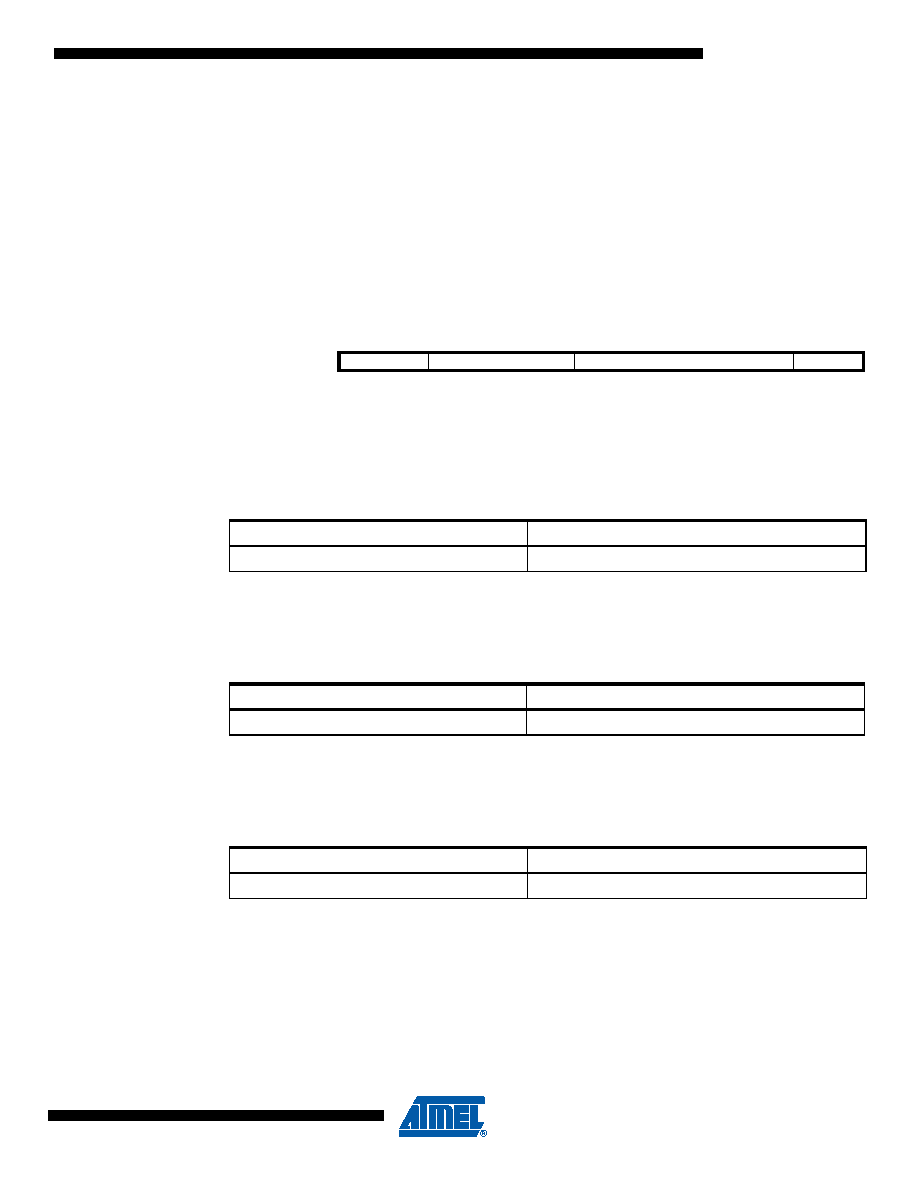
Figure 24-1 shows the structure of the Device Identification Register.
Figure 24-1. The Format of the Device Identification Register
24.3.2.1
Version
Version is a 4-bit number identifying the revision of the component. The JTAG version number
follows the revision of the device. Revision A is 0x0, revision B is 0x1 and so on. However, some
revisions deviate from this rule, and the relevant version number is shown in Table 24-1.
24.3.2.2
Part Number
The part number is a 16-bit code identifying the component. The JTAG Part Number for
ATmega16A is listed in Table 24-2.
24.3.2.3
Manufacturer ID
The Manufacturer ID is a 11 bit code identifying the manufacturer. The JTAG manufacturer ID
for ATMEL is listed in Table 24-3.
24.3.3
Reset Register
The Reset Register is a Test Data Register used to reset the part. Since the AVR tri-states Port
Pins when reset, the Reset Register can also replace the function of the unimplemented optional
JTAG instruction HIGHZ.
A high value in the Reset Register corresponds to pulling the External Reset low. The part is
reset as long as there is a high value present in the Reset Register. Depending on the Fuse set-
tings for the clock options, the part will remain reset for a Reset Time-Out Period (refer to “Clock
MSB
LSB
Bit
31
28
271211
1
0
Device ID
Version
Part Number
Manufacturer ID
1
4 bits
16 bits
11 bits
1 bit
Table 24-1.
JTAG Version Numbers
Version
JTAG Version Number (Hex)
ATmega16A revision TBD
TBD
Table 24-2.
AVR JTAG Part Number
Part Number
JTAG Part Number (Hex)
ATmega16A
0x9403
Table 24-3.
Manufacturer ID
Manufacturer
JTAG Manufacturer ID (Hex)
ATMEL
0x01F
相關(guān)PDF資料 |
PDF描述 |
|---|---|
| R83C154DXXX-12R | 8-BIT, MROM, 12 MHz, MICROCONTROLLER, CQCC44 |
| MR80C32E-12SBR | 8-BIT, 12 MHz, MICROCONTROLLER, CQCC44 |
| IQ80C52EXXX-12D | 8-BIT, MROM, 12 MHz, MICROCONTROLLER, CQFP44 |
| IP80C32-L16:D | 8-BIT, 16 MHz, MICROCONTROLLER, PDIP40 |
| MQ80C52CXXX-25P883 | 8-BIT, MROM, 25 MHz, MICROCONTROLLER, CQFP44 |
相關(guān)代理商/技術(shù)參數(shù) |
參數(shù)描述 |
|---|---|
| IR80C86-2 | 制造商:未知廠家 制造商全稱:未知廠家 功能描述:16-Bit Microprocessor |
| IR80C88 | 制造商:未知廠家 制造商全稱:未知廠家 功能描述:16-Bit Microprocessor |
| IR80C88-2 | 制造商:未知廠家 制造商全稱:未知廠家 功能描述:16-Bit Microprocessor |
| IR-820 | 制造商:BOWEI 制造商全稱:BOWEI 功能描述:Image Rejection Mixers |
| IR8200 | 制造商:IRF 制造商全稱:International Rectifier 功能描述:3A, 55V DMOS H-BRIDGE |
發(fā)布緊急采購,3分鐘左右您將得到回復(fù)。