- 您現(xiàn)在的位置:買賣IC網(wǎng) > PDF目錄383118 > IRFP9150 (HARRIS SEMICONDUCTOR) 25A, 100V, 0.150 Ohm, P-Channel Power MOSFET PDF資料下載
參數(shù)資料
| 型號(hào): | IRFP9150 |
| 廠商: | HARRIS SEMICONDUCTOR |
| 元件分類: | 功率晶體管 |
| 英文描述: | 25A, 100V, 0.150 Ohm, P-Channel Power MOSFET |
| 中文描述: | 25 A, 100 V, 0.15 ohm, P-CHANNEL, Si, POWER, MOSFET, TO-247 |
| 文件頁數(shù): | 2/7頁 |
| 文件大小: | 59K |
| 代理商: | IRFP9150 |
4-64
Absolute Maximum Ratings
T
C
= 25
o
C, Unless Otherwise Specified
IRFP9150
-100
-100
-25
-18
-100
±
20
150
1.2
1300
-55 to 150
UNITS
V
V
A
A
A
V
W
W/
o
C
mJ
o
C
Drain to Source Voltage (Note 1). . . . . . . . . . . . . . . . . . . . . . . . . . . . . . . . . . . . . . . . . . . . . . . . . . . . . . . . . V
DS
Drain to Gate Voltage (R
GS
= 10k
)
(Note 1) . . . . . . . . . . . . . . . . . . . . . . . . . . . . . . . . . . . . . . . . . . . . . .V
DGR
Continuous Drain Current . . . . . . . . . . . . . . . . . . . . . . . . . . . . . . . . . . . . . . . . . . . . . . . . . . . . . . . . . . . . . . . .I
D
T
C
=100
o
C . . . . . . . . . . . . . . . . . . . . . . . . . . . . . . . . . . . . . . . . . . . . . . . . . . . . . . . . . . . . . . . . . . . . . . . . . .I
D
Pulsed Drain Current . . . . . . . . . . . . . . . . . . . . . . . . . . . . . . . . . . . . . . . . . . . . . . . . . . . . . . . . . . . . . . . . . . I
DM
Gate to Source Voltage . . . . . . . . . . . . . . . . . . . . . . . . . . . . . . . . . . . . . . . . . . . . . . . . . . . . . . . . . . . . . . . . V
GS
Maximum Power Dissipation . . . . . . . . . . . . . . . . . . . . . . . . . . . . . . . . . . . . . . . . . . . . . . . . . . . . . . . . . . . . . P
D
Linear Derating Factor . . . . . . . . . . . . . . . . . . . . . . . . . . . . . . . . . . . . . . . . . . . . . . . . . . . . . . . . . . . . . . . . . . . .
Single Pulse Avalanche Energy Rating (Note 3) . . . . . . . . . . . . . . . . . . . . . . . . . . . . . . . . . . . . . . . . . . . . . E
as
Operating and Storage Temperature . . . . . . . . . . . . . . . . . . . . . . . . . . . . . . . . . . . . . . . . . . . . . . . . . . T
J
, T
STG
Maximum Temperature for Soldering
Leads at 0.063in (1.6mm) from Case for 10s. . . . . . . . . . . . . . . . . . . . . . . . . . . . . . . . . . . . . . . . . . . . . . . T
L
Package Body for 10s, See Techbrief 334 . . . . . . . . . . . . . . . . . . . . . . . . . . . . . . . . . . . . . . . . . . . . . . . .T
pkg
300
260
o
C
o
C
CAUTION: Stresses above those listed in “Absolute Maximum Ratings” may cause permanent damage to the device. This is a stress only rating and operation of the
device at these or any other conditions above those indicated in the operational sections of this specification is not implied.
NOTE:
1. T
J
= 25
o
C to 125
o
C
Electrical Specifications
T
C
= 25
o
C, Unless Otherwise Specified
PARAMETER
SYMBOL
TEST CONDITIONS
MIN
TYP
MAX
UNITS
Drain to Source Breakdown Voltage
BV
DSS
V
GS(TH)
I
DSS
V
GS
= 0V, I
D
= -250
μ
A (Figure 10)
V
DS
= V
GS
, I
D
= -250
μ
A
V
DS
= Rated BV
DSS
, V
GS
= 0V
V
DS
= 0.8 x Rated BV
DSS
, V
GS
= 0V, T
C
= 125
o
C
1
-
-
V
Gate Threshold Voltage
-2.0
-
-4.0
V
Zero Gate Voltage Drain Current
-
-
25
μ
A
μ
A
-
-
250
On-State Drain Current (Note 2)
I
D(ON)
V
DS
> I
D(ON)
x
r
DS(ON)MAX,
V
GS
= 10V
V
GS
=
±
20V
V
GS
= -10V, I
D
= -10A (Figure 8, 9)
V
DS
≤
-10V, I
D
= -12.5A (Figure 12)
V
DD
= -50V, I
D
≈
-25A, R
G
= 6.8
, R
L
= 2
(Figures 17 and 18) MOSFET switching times are es-
sentially independent of operating temperature).
-25
-
-
A
Gate to Source Leakage Current
I
GSS
r
DS(ON)
g
fs
t
d(ON)
t
r
t
d(OFF)
t
f
Q
g(TOT)
-
±
100
nA
Drain to Source On Resistance (Note 2)
-
0.090
0.150
Forward Transconductance (Note 2)
4
10
-
S
Turn-On Delay Time
-
16
24
ns
Rise Time
-
110
160
ns
Turn-Off Delay Time
-
65
100
ns
Fall Time
-
46
70
ns
Total Gate Charge
(Gate to Source + Gate to Drain)
V
GS
= -10V, I
D
= -25A, V
DS
= 0.8 x Rated BV
DSS
I
g(REF)
= -1.5mA (Figures 14, 19, 20)
(Gate Charge is Essentially Independent Of Operat-
ing Temperature)
-
82
120
nC
Gate to Source Charge
Q
gs
Q
gd
C
ISS
C
OSS
C
RSS
L
D
-
14
-
nC
Gate to Drain “Miller” Charge
-
42
-
nC
Input Capacitance
V
GS
= 0V, V
DS
= -25V, f = 1.0MHz
(Figure 11)
-
2400
-
pF
Output Capacitance
-
850
-
pF
Reverse Transfer Capacitance
-
400
-
pF
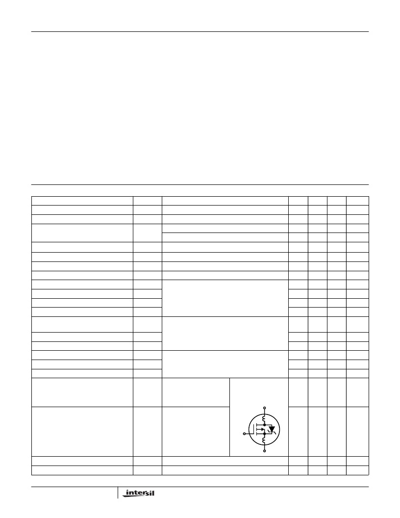
Internal Drain Inductance
Measured From the Drain
Lead, 6mm (0.25in) From
the Package to the Center
of the Die
Modified MOSFET
Symbol Showing the In-
ternal Device Induc-
tances
-
5.0
-
nH
Internal Source Inductance
L
S
MeasuredFromtheSource
Pin, 6mm (0.25in) From
Header to the Source
Bonding Pad
-
13
-
nH
Thermal Resistance Junction to Case
R
θ
JC
R
θ
JA
-
-
0.83
o
C/W
Thermal Resistance Junction to Ambient
Free Air Operation
-
-
30
0
C/W
L
S
L
D
G
D
S
IRFP9150
相關(guān)PDF資料 |
PDF描述 |
|---|---|
| IRFR220 | 4.6A, 200V, 0.800 Ohm,N-Channel PowerMOSFET(4.6A, 200V, 0.800 Ω,nN溝道增強(qiáng)型功率MOS場(chǎng)效應(yīng)管) |
| IRFU220 | 4.6A, 200V, 0.800 Ohm, N-Channel Power MOSFETs |
| IRFR420 | 2.5A, 500V, 3.000 Ohm, N-Channel Power MOSFETs(2.5A, 500V, 3.000 Ω, N溝道功率MOS場(chǎng)效應(yīng)管) |
| IRFU420 | 2.5A, 500V, 3.000 Ohm, N-Channel Power MOSFETs |
| IRFU420 | Power MOSFET(Vdss=500V, Rds(on)=3.0ohm, Id=2.4A) |
相關(guān)代理商/技術(shù)參數(shù) |
參數(shù)描述 |
|---|---|
| IRFP9150_R4941 | 功能描述:MOSFET TO-247 RoHS:否 制造商:STMicroelectronics 晶體管極性:N-Channel 汲極/源極擊穿電壓:650 V 閘/源擊穿電壓:25 V 漏極連續(xù)電流:130 A 電阻汲極/源極 RDS(導(dǎo)通):0.014 Ohms 配置:Single 最大工作溫度: 安裝風(fēng)格:Through Hole 封裝 / 箱體:Max247 封裝:Tube |
| IRFP9151 | 制造商:未知廠家 制造商全稱:未知廠家 功能描述:TRANSISTOR | MOSFET | P-CHANNEL | 60V V(BR)DSS | 25A I(D) | TO-247 |
| IRFP9230 | 制造商:SAMSUNG 制造商全稱:Samsung semiconductor 功能描述:P-CHANNEL POWER MOSFETS |
| IRFP9231 | 制造商:SAMSUNG 制造商全稱:Samsung semiconductor 功能描述:P-CHANNEL POWER MOSFETS |
| IRFP9232 | 制造商:SAMSUNG 制造商全稱:Samsung semiconductor 功能描述:P-CHANNEL POWER MOSFETS |
發(fā)布緊急采購,3分鐘左右您將得到回復(fù)。