- 您現(xiàn)在的位置:買賣IC網(wǎng) > PDF目錄377523 > IRIS-A6131 (International Rectifier) INTEGRATED SWITCHER PDF資料下載
參數(shù)資料
| 型號: | IRIS-A6131 |
| 廠商: | International Rectifier |
| 英文描述: | INTEGRATED SWITCHER |
| 中文描述: | 多功能開關(guān) |
| 文件頁數(shù): | 3/7頁 |
| 文件大小: | 396K |
| 代理商: | IRIS-A6131 |
www.irf.com 3
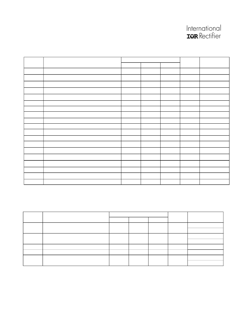
Electrical Characteristics (for Control IC)
Electrical characteristics for control part (Ta=25
℃
, Vin=20V,unless otherwise specified)
MIN
16
9
-
-
9.6
0.2
7.3
0.69
200
0.7
6.5
18
227
340
-
28.7
-
TYP
17.5
10
-
-
10.6
-
8
0.77
320
0.79
7.2
26
300
790
-
31.2
-
MAX
19.2
11
4
50
11.6
-
8.7
0.86
480
0.88
7.9
35
388
1230
30
34.1
200
V
CC
(ON)
V
CC
(OFF)
I
CC
(ON)
I
CC
(OFF)
V
CC
(bias)
-
T
OFF(MAX)
Maximum OFF time
V
OCP
O.C.P. threshold voltage
Tbw
Leading edge blanking time
Vburst
Burst threshold voltage
V
OLP
O.L.P. threshold voltage
I
OLP
Out-flow current at O.L.P operation
I
FB(MAX)
Maximum F.B. current
I
STARTUP
Startup current
I
START(leak)
Startup circuit leakage current
V
CC
(OVP)
O.V.P operation voltage
I
CC(H)
Latch circuit sustaining current *6
Operation start voltage
Operation stop voltage
Circuit current in operation
Circuit current in non-operation
Auto bias threshold voltage
Vcc(bias) - Vcc(OFF)
V
V
VCC=0
→
19.2V
VCC=19.2
→
9.V
mA
μA
V
V
μsec
V
nsec
V
V
μA
μA
μA
μA
V
μA
-
VCC=14V
VCC=20
→
9.6V
-
-
-
-
-
-
-
-
VCC=15V
-
VCC=0
→
34.1V
V
CC
(La.OFF)
Latch circuit release voltage *6
Tj
(TSD)
Thermal shutdown operating temperature
6.6
135
7.3
-
8
-
V
℃
VCC=34.1
→
6.6
V
-
Ratings
VCC=34.1
→
8.5V
Units
Test
Conditions
Definition
Symbol
Electrical Characteristics (for MOSFET)
(Ta=25
℃
) unless otherwise specified
*6 The latch circuit means a circuit operated O.V.P and T.S.D.
MIN
TYP
MAX
ID=300μA
V1
-3
=0V(short)
V
DS
=500V
V1
-3
=0V(short)
R
DS(ON)
tf
On-resistance
Switching time
-
-
-
-
3.95
250
Ω
nsec
I
D
=0.4A
-
Between channel and
internal frame
Ratings
Units
Test Conditions
Drain-to-Source breakdown voltage
V
DSS
500
-
-
V
Definition
Symbol
μA
Drain leakage current
I
DSS
-
θ
ch-F
-
-
300
-
52
℃
/W
Thermal resistance *7
*7 Internal frame temperature (T
F
) is measured at the root of the Pin 3.
IRIS-A6131
相關(guān)PDF資料 |
PDF描述 |
|---|---|
| IRISa6331 | INTEGRATED SWITCHER |
| IRK.236 | STANDARD RECOVERY DIODES |
| IRKD236-04 | STANDARD RECOVERY DIODES |
| IRK166 | STANDARD RECOVERY DIODES |
| IRK.166 | STANDARD RECOVERY DIODES |
相關(guān)代理商/技術(shù)參數(shù) |
參數(shù)描述 |
|---|---|
| IRIS-A6151 | 制造商:IRF 制造商全稱:International Rectifier 功能描述:INTEGRATED SWITCHER |
| IRIS-A6159 | 制造商:IRF 制造商全稱:International Rectifier 功能描述:INTEGRATED SWITCHER |
| IRISA6331 | 制造商:IRF 制造商全稱:International Rectifier 功能描述:INTEGRATED SWITCHER |
| IRIS-A6331 | 制造商:IRF 制造商全稱:International Rectifier 功能描述:INTEGRATED SWITCHER |
| IRIS-A6351 | 制造商:IRF 制造商全稱:International Rectifier 功能描述:INTEGRATED SWITCHER |
發(fā)布緊急采購,3分鐘左右您將得到回復。