- 您現(xiàn)在的位置:買賣IC網(wǎng) > PDF目錄377534 > IRL5NJ024 (International Rectifier) LOGIC LEVEL HEXFET POWER MOSFET SURFACE MOUNT (SMD-0.5) PDF資料下載
參數(shù)資料
| 型號: | IRL5NJ024 |
| 廠商: | International Rectifier |
| 英文描述: | LOGIC LEVEL HEXFET POWER MOSFET SURFACE MOUNT (SMD-0.5) |
| 中文描述: | 邏輯電平HEXFET功率MOSFET的表面貼裝系統(tǒng)(SMD - 0.5) |
| 文件頁數(shù): | 2/7頁 |
| 文件大小: | 115K |
| 代理商: | IRL5NJ024 |
IRL5NJ024
2
www.irf.com
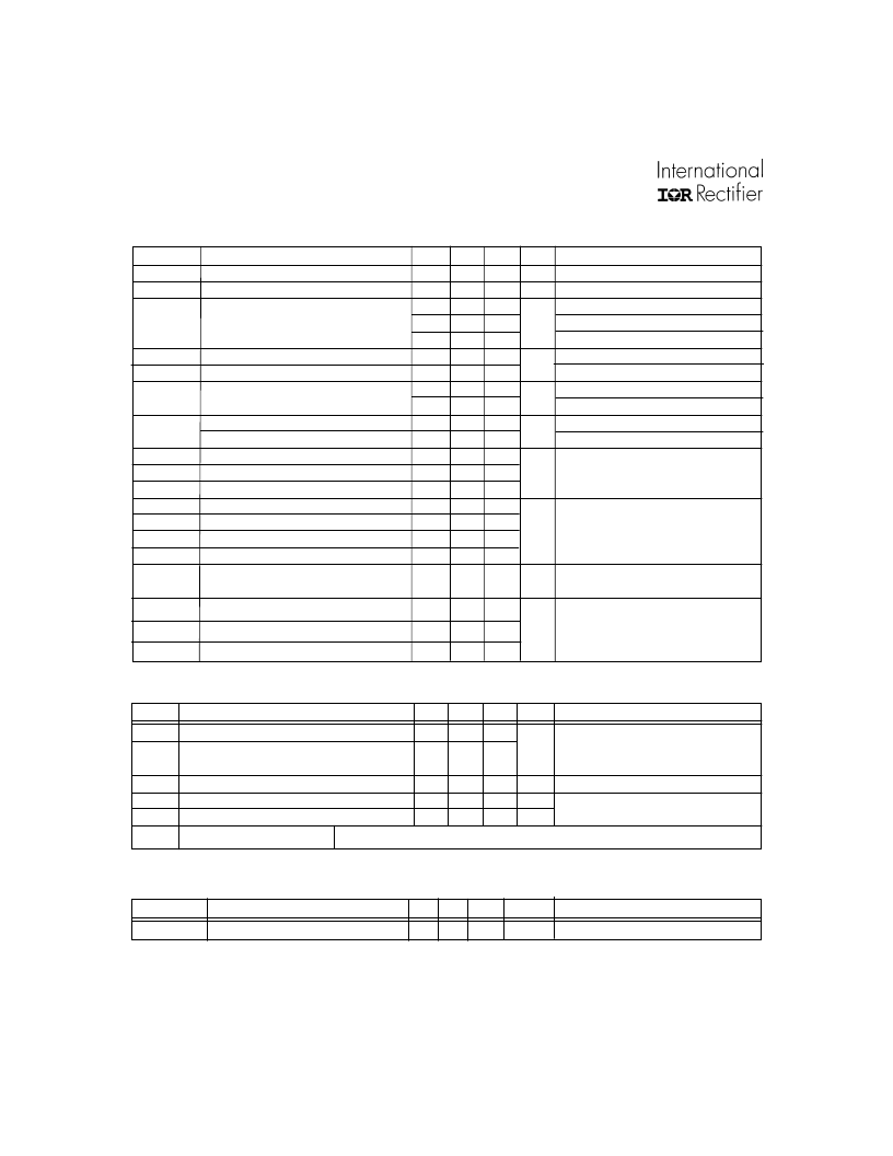
Thermal Resistance
Parameter
RthJC
Junction-to-Case
Min Typ Max
—
—
Units
Test Conditions
3.57
°C/W
Source-Drain Diode Ratings and Characteristics
Parameter
IS
Continuous Source Current (Body Diode)
ISM
Pulse Source Current (Body Diode)
Min Typ
—
—
Max Units
17
68
Test Conditions
—
—
VSD
trr
QRR
ton
Diode Forward Voltage
Reverse Recovery Time
Reverse Recovery Charge
—
—
—
—
—
—
1.3
90
200
V
nS
nC
T
j
= 25°C, IS = 11A, VGS = 0V
Tj = 25°C, IF = 11A, di/dt
≤
100A/
μ
s
VDD
≤
25V
Forward Turn-On Time
Intrinsic turn-on time is negligible. Turn-on speed is substantially controlled by LS + LD.
A
Note: Corresponding Spice and Saber models are available on the G&S Website.
For footnotes refer to the last page
Parameter
Min. Typ. Max. Units
55
–––
–––
0.057 –––
–––
––– 0.060
–––
––– 0.075
–––
––– 0.105
1.0
–––
6.5
–––
–––
–––
–––
–––
–––
–––
–––
–––
–––
–––
–––
–––
–––
–––
–––
–––
–––
–––
–––
–––
–––
–––
–––
4.0 ––– nH
Conditions
V
GS
= 0V, I
D
= 250μA
Reference to 25°C, I
D
= 1mA
V
GS
= 10V, I
D
= 11A
V
GS
= 5.0V, I
D
= 11A
V
GS
= 4.0V, I
D
= 9.0A
V
DS
= V
GS
, I
D
= 250μA
V
DS
= 25V, I
D
= 11 A
V
DS
= 55V, V
GS
= 0V
V
DS
= 44V, V
GS
= 0V, T
J
= 125°C
V
GS
= 16V
V
GS
= -16V
I
D
= 11A
V
DS
= 44V
V
GS
= 5.0V
V
DD
= 28V
I
D
= 11A
R
G
= 12
V
GS
= 5.0V
Measured from the center of
V
(BR)DSS
V
(BR)DSS
/
T
J
Breakdown Voltage Temp. Coefficient
Drain-to-Source Breakdown Voltage
–––
V
V/°C
V
GS(th)
g
fs
Gate Threshold Voltage
Forward Transconductance
2.0
–––
25
250
100
-100
15
3.7
8.5
11
133
35
66
V
S
μA
Gate-to-Source Forward Leakage
Gate-to-Source Reverse Leakage
Total Gate Charge
Gate-to-Source Charge
Gate-to-Drain ("Miller") Charge
Turn-On Delay Time
Rise Time
Turn-Off Delay Time
Fall Time
Total Inductance
drain pad to center of source pad
Input Capacitanc
–––
514
nA
Q
g
Q
gs
Q
gd
t
d(on)
t
r
t
d(off)
t
f
LS + LD
nC
ns
C
iss
–––
V
GS
= 0V, V
DS
= 25V
Electrical Characteristics @ T
J
= 25°C (unless otherwise specified)
I
GSS
R
DS(on)
Static Drain-to-Source On-Resistance
I
DSS
Drain-to-Source Leakage Current
C
rss
Reverse Transfer Capacitance
–––
51
–––
C
oss
Output Capacitance
–––
137
–––
pF
= 1.0MHz
相關(guān)PDF資料 |
PDF描述 |
|---|---|
| IRL640 | HEXFET Power MOSFET(HEXFET 功率MOS場效應(yīng)管) |
| IRL8113LPBF | HEXFET Power MOSFET |
| IRL8113PBF | HEXFET Power MOSFET |
| IRL8113SPBF | HEXFET Power MOSFET |
| IRL8113 | HEXFET Power MOSFET |
相關(guān)代理商/技術(shù)參數(shù) |
參數(shù)描述 |
|---|---|
| IRL5NJ024SCV | 制造商:International Rectifier 功能描述:TRANS MOSFET N-CH 55V 17A 3SMD-0.5 - Bulk |
| IRL5NJ024SCX | 制造商:International Rectifier 功能描述:TRANS MOSFET N-CH 55V 17A 3SMD-0.5 - Bulk |
| IRL5NJ5305 | 制造商:International Rectifier 功能描述:P-FET SMD- 0.5 PKG - Bulk |
| IRL5NJ7404 | 制造商:International Rectifier 功能描述: |
| IRL5NJ7404SCV | 制造商:International Rectifier 功能描述:TRANS MOSFET P-CH 20V 11A 3SMD-0.5 - Bulk |
發(fā)布緊急采購,3分鐘左右您將得到回復(fù)。