- 您現(xiàn)在的位置:買賣IC網(wǎng) > PDF目錄16308 > ISL36411DRZ-EVALZ (Intersil)EVAL BOARD FOR ISL36411DRZ PDF資料下載
參數(shù)資料
| 型號: | ISL36411DRZ-EVALZ |
| 廠商: | Intersil |
| 文件頁數(shù): | 6/12頁 |
| 文件大小: | 0K |
| 描述: | EVAL BOARD FOR ISL36411DRZ |
| 標(biāo)準(zhǔn)包裝: | 1 |
| 系列: | * |

ISL36411
3
FN6965.1
March 25, 2010
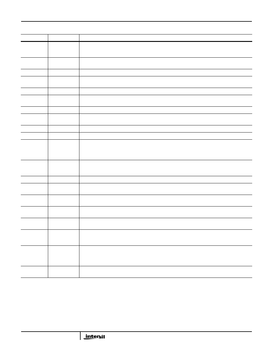
Pin Functions and Definitions
PIN NAME
PIN NUMBER
DESCRIPTION
VDD
1, 5, 9, 13, 24,
27, 28, 31, 32,
35, 36, 39
Power supply. 1.2V supply voltage. The use of parallel 100pF and 10nF decoupling capacitors to
ground is recommended for each of these pins for broad high-frequency noise suppression.
IN1[P, N]
2, 3
Equalizer 1 differential input, CML. the use of 100nF low ESL/ESR MLCC capacitor with at least
6GHz frequency response is recommended.
LOSB1
4
LOS BAR indicator 1. Low output when IN1 signal is below DT threshold.
IN2[P, N]
6, 7
Equalizer 2 differential input, CML. the use of 100nF low ESL/ESR MLCC capacitor with at least
6GHz frequency response is recommended.
LOSB2
8
LOS BAR indicator 2. Low output when IN2 signal is below DT threshold.
IN3[P, N]
10, 11
Equalizer 3 differential input, CML. the use of 100nF low ESL/ESR MLCC capacitor with at least
6GHz frequency response is recommended.
LOSB3
12
LOS BAR indicator 3. Low output when IN3 signal is below DT threshold.
IN4[P, N]
14, 15
Equalizer 4 differential input, CML. the use of 100nF low ESL/ESR MLCC capacitor with at least
6GHz frequency response is recommended.
LOSB4
16
LOS BAR indicator 4. Low output when IN4 signal is below DT threshold.
GND
17, 23, 40, 46 These pins should be grounded.
DT2
18
Detection Threshold for equalizers 3 and 4. Reference DC voltage threshold for input signal
power detection. Data output OUT3 and OUT4 are muted when the power of IN3 and IN4,
respectively, fall below the threshold. Tie to ground to disable electrical idle preservation and
always enable the limiting amplifier.
CP2[A,B]
19, 20
Control pins for setting equalizers 3 and 4. CMOS logic inputs. Pins are read as a 2-digit number
to set the boost level. A is the MSB, and B is the LSB. Pins are internally pulled down through a
25kΩ resistor.
NC
21, 22, 41, 45 not connected: do not make any connections to these pins.
OUT4[N, P]
25, 26
Equalizer 4 differential output, CML. The use of 100nF low ESL/ESR MLCC capacitor with at least
6GHz frequency response is recommended.
OUT3[N, P]
29, 30
Equalizer 3 differential output, CML. The use of 100nF low ESL/ESR MLCC capacitor with at least
6GHz frequency response is recommended.
OUT2[N, P]
33, 34
Equalizer 2 differential output, CML. The use of 100nF low ESL/ESR MLCC capacitor with at least
6GHz frequency response is recommended.
OUT1[N, P]
37, 38
Equalizer 1 differential output, CML. The use of 100nF low ESL/ESR MLCC capacitor with at least
6GHz frequency response is recommended.
CP1[B, A]
42, 43
Control pins for setting equalizers 1 and 2. CMOS logic inputs. Pins are read as a 2-digit number
to set the boost level. A is the MSB, and B is the LSB. Pins are internally pulled down through a
25kΩ resistor.
DT1
44
Detection Threshold for equalizers 1 and 2. Reference DC voltage threshold for input signal
power detection. Data output OUT1 and OUT2 are muted when the power of IN1 and IN2,
respectively, fall below the threshold. Tie to ground to disable electrical idle preservation and
always enable the limiting amplifier.
Exposed Pad
-
Exposed ground pad. For proper electrical and thermal performance, this pad should be
connected to the PCB ground plane.
相關(guān)PDF資料 |
PDF描述 |
|---|---|
| EEM40DTAH-S189 | CONN EDGECARD 80POS R/A .156 SLD |
| EEM40DTAD-S189 | CONN EDGECARD 80POS R/A .156 SLD |
| ISL36111DRZ-EVALZ | EVAL BOARD FOR ISL36111DRZ |
| M3CKK-1620K | IDC CABLE - MKC16K/MC16F/MPK16K |
| ISL35411DRZ-EVALZ | EVAL BAORD FOR ISL35411DRZ |
相關(guān)代理商/技術(shù)參數(shù) |
參數(shù)描述 |
|---|---|
| ISL36411DRZ-T7 | 功能描述:接口 - 專用 ISL54100AHDMI EVAL BRD RHS CMPL 12 8LD RoHS:否 制造商:Texas Instruments 產(chǎn)品類型:1080p60 Image Sensor Receiver 工作電源電壓:1.8 V 電源電流:89 mA 最大功率耗散: 最大工作溫度:+ 85 C 安裝風(fēng)格:SMD/SMT 封裝 / 箱體:BGA-59 |
| ISL36411DRZ-TS | 功能描述:接口 - 專用 ISL54065 EVALRD 1 SOCKET DGHTR BRD- 1 RoHS:否 制造商:Texas Instruments 產(chǎn)品類型:1080p60 Image Sensor Receiver 工作電源電壓:1.8 V 電源電流:89 mA 最大功率耗散: 最大工作溫度:+ 85 C 安裝風(fēng)格:SMD/SMT 封裝 / 箱體:BGA-59 |
| ISL3680 | 制造商:INTERSIL 制造商全稱:Intersil Corporation 功能描述:Direct Conversion Transceiver |
| ISL3680IR | 制造商:INTERSIL 制造商全稱:Intersil Corporation 功能描述:Direct Conversion Transceiver |
| ISL3680IR-TK | 制造商:INTERSIL 制造商全稱:Intersil Corporation 功能描述:Direct Conversion Transceiver |
發(fā)布緊急采購,3分鐘左右您將得到回復(fù)。