- 您現(xiàn)在的位置:買賣IC網(wǎng) > PDF目錄383156 > ISL6557CB (INTERSIL CORP) PWM Controller with Wide Input Voltage Range 8-PDIP -20 to 85 PDF資料下載
參數(shù)資料
| 型號: | ISL6557CB |
| 廠商: | INTERSIL CORP |
| 元件分類: | 穩(wěn)壓器 |
| 英文描述: | PWM Controller with Wide Input Voltage Range 8-PDIP -20 to 85 |
| 中文描述: | SWITCHING CONTROLLER, 1500 kHz SWITCHING FREQ-MAX, PDSO24 |
| 封裝: | PLASTIC, MS-013AD, SOIC-24 |
| 文件頁數(shù): | 5/17頁 |
| 文件大?。?/td> | 532K |
| 代理商: | ISL6557CB |
5
NOTES:
2. These parts are designed and adjusted for accuracy within the system tolerance given in the Electrical Specifications. The system tolerance
accounts for offsets in the differential and error amplifiers; reference-voltage inaccuracies; temperature drift; and the full DAC adjustment range.
3. VID input levels above 2.9V may produce an reference-voltage offset inaccuracy.
Functional Pin Descriptions
VID4, VID3, VID2, VID1, VID0 (Pins 1, 2, 3, 4, 5)
These are the inputs to the internal DAC that provides the
reference voltage for output regulation. Connect these pins
to either open-drain or active-pull-up type outputs. Pulling
these pins above 2.9V can cause a reference offset
inaccuracy.
FB (Pin 7) and COMP (Pin 6)
The internal error amplifier’s inverting input and output
respectively. These pins are connected to an external R-C
network to compensate the regulator.
IOUT (Pin 8)
The current out of this pin is proportional to output current
and is used for load-line regulation and load sharing. The
scale factor is set by the ratio of the ISEN resistors
(connected to pins 14, 15, 18, and 19) to the lower
MOSFET
r
DS(ON)
.
VDIFF (Pin 9), VSEN (Pin 10), RGND (Pin 11)
VSEN and RGND are the inputs to the differential remote-
sense amplifier. VDIFF is the output and it serves as the
input to the external regulation circuitry and the internal
protection circuitry. Connect VSEN and RGND to the sense
pins of the remote load.
GND (Pin 12)
Return for VCC and signal ground for the IC.
PWM3, PWM2, PWM1, PWM4 (Pins 13, 16, 17, 20)
Pulse-width modulation outputs. These logic outputs tell the
driver IC(s) when to turn the MOSFETs on and off.
ISEN3, ISEN2, ISEN1, ISEN4 (PINS 14, 15, 18, 19)
Current sense inputs. A resistor connected between these
pins and the respective phase nodes has a current
proportional to the current in the lower MOSFET during its
conduction interval. The current is used as a reference for
channel balancing, load sharing, protection, and load-line
regulation.
PGOOD (Pin 21)
PGOOD is an open-drain logic output that changes to a logic
low when the differential output voltage at VDIFF swings
below 0.9V or above 2.1V.
FS (Pin 22)
This pin has two functions. A resistor placed from FS to
ground sets the switching frequency. There is an inverse
relationship between the value of the resistor and the
switching frequency. This pin can also be used to disable the
controller. To disable the controller, pull this pin below 1V.
EN (Pin 23)
This is the threshold-sensitive enable input for the controller.
To enable the controller, pull this pin above 1.23V.
VCC (Pin 24)
Bias supply voltage for the controller. Connect this pin to a
5V power supply.
ISEN
Overcurrent Trip Level
-90
-75
-60
μ
A
PROTECTION and MONITOR
Overvoltage Threshold
VSEN Rising
2.04
2.09
2.13
V
VSEN Falling
VID
V
Undervoltage Threshold
VSEN Rising
0.810
0.990
V
VSEN Falling
0.835
0.925
V
PGOOD Low Voltage
IPGOOD = 4mA
0.18
0.4
mV
Electrical Specifications
Operating Conditions: V
CC
= 5V, T
A
= 0
o
C to 70
o
C, Unless Otherwise Specified
(Continued)
PARAMETER
TEST CONDITIONS
MIN
TYP
MAX
UNITS
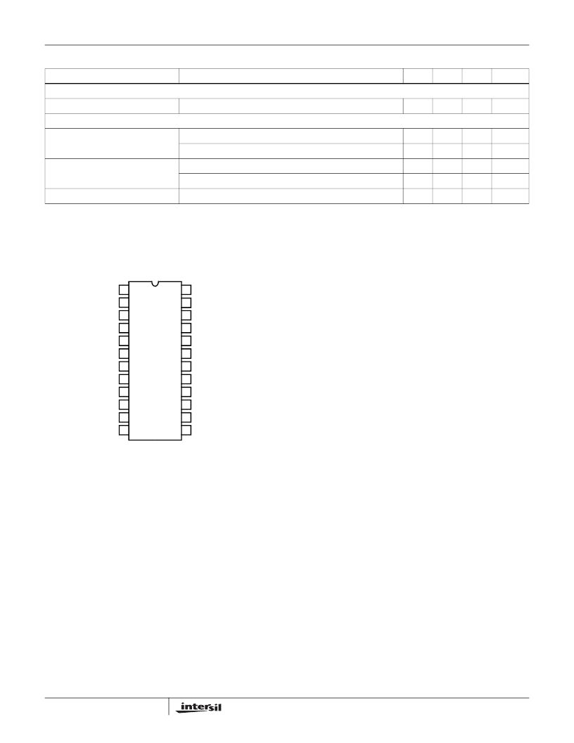
VID4
VID3
VID2
VID1
VID0
IOUT
PWM2
PGOOD
PWM3
ISEN4
ISEN1
VDIFF
ISEN3
FB
PWM4
VSEN
COMP
PWM1
ISEN2
RGND
GND
FS
EN
VCC
1
2
3
4
5
6
7
8
9
10
11
12
13
14
15
16
17
18
19
20
21
22
23
24
ISL6557
相關(guān)PDF資料 |
PDF描述 |
|---|---|
| ISL6558CRZA-T | Multi-Purpose Precision Multi-Phase PWM Controller With Optional Active Voltage Positioning |
| ISL6558IB | Multi-Purpose Precision Multi-Phase PWM Controller With Optional Active Voltage Positioning |
| ISL6558IB-T | Multi-Purpose Precision Multi-Phase PWM Controller With Optional Active Voltage Positioning |
| ISL6558IBZ | Multi-Purpose Precision Multi-Phase PWM Controller With Optional Active Voltage Positioning |
| ISL6558IBZ-T | Multi-Purpose Precision Multi-Phase PWM Controller With Optional Active Voltage Positioning |
相關(guān)代理商/技術(shù)參數(shù) |
參數(shù)描述 |
|---|---|
| ISL6557CB-T | 制造商:Intersil Corporation 功能描述: |
| ISL6557CB-T WAF | 制造商:Intersil Corporation 功能描述: |
| ISL6558CB | 功能描述:DC/DC 開關(guān)控制器 Precision MultiPhase RoHS:否 制造商:Texas Instruments 輸入電壓:6 V to 100 V 開關(guān)頻率: 輸出電壓:1.215 V to 80 V 輸出電流:3.5 A 輸出端數(shù)量:1 最大工作溫度:+ 125 C 安裝風格: 封裝 / 箱體:CPAK |
| ISL6558CB-T | 功能描述:IC REG CTRLR BUCK PWM 16-SOIC RoHS:否 類別:集成電路 (IC) >> PMIC - 穩(wěn)壓器 - DC DC 切換控制器 系列:- 標準包裝:4,000 系列:- PWM 型:電壓模式 輸出數(shù):1 頻率 - 最大:1.5MHz 占空比:66.7% 電源電壓:4.75 V ~ 5.25 V 降壓:是 升壓:無 回掃:無 反相:無 倍增器:無 除法器:無 Cuk:無 隔離:無 工作溫度:-40°C ~ 85°C 封裝/外殼:40-VFQFN 裸露焊盤 包裝:帶卷 (TR) |
| ISL6558CBZ | 制造商:Intersil Corporation 功能描述:- Rail/Tube |
發(fā)布緊急采購,3分鐘左右您將得到回復。