- 您現(xiàn)在的位置:買賣IC網(wǎng) > PDF目錄383198 > IXGH32N50B (IXYS CORP) HiPerFAST IGBT PDF資料下載
參數(shù)資料
| 型號(hào): | IXGH32N50B |
| 廠商: | IXYS CORP |
| 元件分類: | IGBT 晶體管 |
| 英文描述: | HiPerFAST IGBT |
| 中文描述: | 60 A, 500 V, N-CHANNEL IGBT, TO-247AD |
| 封裝: | TO-247AD, 3 PIN |
| 文件頁(yè)數(shù): | 2/2頁(yè) |
| 文件大小: | 50K |
| 代理商: | IXGH32N50B |
IXYS MOSFETS and IGBTs are covered by one or more of the following U.S. patents:
4,835,592
4,850,072
4,881,106
4,931,844
5,017,508
5,034,796
5,049,961
5,063,307
5,187,117
5,237,481
5,486,715
5,381,025
IXYS reserves the right to change limits, test conditions, and dimensions.
IXGH32N50B
IXGH32N50BS
Inductive load, T
J
= 25
°
C
I
C
= I
, V
GE
= 15 V, L = 100
μ
H,
V
CE
= 0.8 V
CES
, R
G
= R
off
= 4.7
Remarks: Switching times may
increase for V
(Clamp) > 0.8 V
CES
,
higher T
J
or increased R
G
Inductive load, T
J
= 125
°
C
I
C
= I
C90
, V
GE
= 15 V, L = 100
μ
H
V
CE
= 0.8 V
CES
, R
G
= R
off
= 4.7
Remarks: Switching times may
increase for V
(Clamp) > 0.8 V
CES
,
higher T
J
or increased R
G
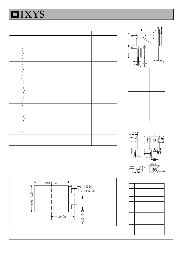
Dim.
Millimeter
Min.
4.7
2.2
2.2
1.0
1.65
2.87
.4
20.80
15.75
5.20
19.81
Inches
Min.
.185
.087
.059
.040
.065
.113
.016
.819
.610
0.205 0.225
.780
Max.
5.3
2.54
2.6
1.4
2.13
3.12
Max.
.209
.102
.098
.055
.084
.123
.031
.845
.640
A
A
1
A
2
b
b
1
b
2
C
D
E
e
L
L1
P
Q
R
S
.8
21.46
16.26
5.72
20.32
4.50
3.65
6.40
5.49
.800
.177
.144
3.55
5.89
4.32
6.15 BSC
.140
0.232 0.252
.170
242 BSC
.216
e
P
1. Gate
2. Collector
3. Emitter
4. Collector
Dim.
Millimeter
Min.
4.83
2.29
1.91
1.14
1.91
0.61
20.80
15.75
5.45
4.90
2.70
2.10
0.00
1.90
3.55
5.59
4.32
6.15
Inches
Min.
.190
.090
.075
.045
.075
.024
.819
.620
.215
.193
.106
.083
.00
.075
.140
.220
.170
.242
Max.
5.21
2.54
2.16
1.40
2.13
0.80
21.34
16.13
BSC
5.10
2.90
2.30
0.10
2.10
3.65
6.20
4.83
BSC
Max.
.205
.100
.085
.055
.084
.031
.840
.635
BSC
.201
.114
.091
.004
.083
.144
.244
.190
BSC
A
A1
A2
b
b1
C
D
E
e
L
L1
L2
L3
L4
P
Q
R
S
Symbol
Test Conditions
Characteristic Values
(T
J
= 25
°
C, unless otherwise specified)
min.
typ.
max.
g
fs
I
Pulse test, t
≤
300
μ
s, duty cycle
≤
2 %
= I
; V
CE
= 10 V,
15
20
S
C
ies
C
oes
C
res
2500
230
pF
pF
pF
V
CE
= 25 V, V
GE
= 0 V, f = 1 MHz
70
Q
g
Q
ge
Q
gc
125
23
50
150
35
75
nC
nC
nC
I
C
= I
C90
, V
GE
= 15 V, V
CE
= 0.5 V
CES
t
d(on)
t
ri
t
d(off)
t
fi
E
off
25
30
ns
ns
ns
ns
mJ
100
80
0.7
200
150
1.5
t
d(on)
t
ri
E
on
t
d(off)
t
fi
25
35
0.3
120
120
ns
ns
mJ
ns
ns
E
off
1.2
mJ
R
thJC
R
thCK
0.62 K/W
0.25
K/W
TO-247 AD Outline
TO-247 SMD Outline
Min. Recommended Footprint
(Dimensions in inches and (mm))
相關(guān)PDF資料 |
PDF描述 |
|---|---|
| IXGH32N50BS | HiPerFAST IGBT |
| IXGH32N60AU1 | HiPerFAST IGBT with Diode(VCES為600V,VCE(sat)為2.9V的HiPerFAST絕緣柵雙極晶體管(帶二極管)) |
| IXGH32N60A | HiPerFAST IGBT |
| IXGH32N60AS | HiPerFAST IGBT |
| IXGH32N60BD1 | Connector Cover; Number of Contacts:1; Color:Red; Contact Termination:Crimp or Solder |
相關(guān)代理商/技術(shù)參數(shù) |
參數(shù)描述 |
|---|---|
| IXGH32N50BS | 制造商:IXYS 制造商全稱:IXYS Corporation 功能描述:HiPerFAST IGBT |
| IXGH32N50BU1 | 制造商:IXYS 制造商全稱:IXYS Corporation 功能描述:HiPerFAST IGBT with Diode Combi Pack |
| IXGH32N50BU1S | 制造商:IXYS 制造商全稱:IXYS Corporation 功能描述:HiPerFAST IGBT with Diode Combi Pack |
| IXGH32N60A | 制造商:IXYS 制造商全稱:IXYS Corporation 功能描述:HiPerFAST IGBT |
| IXGH32N60AS | 制造商:IXYS 制造商全稱:IXYS Corporation 功能描述:HiPerFAST IGBT |
發(fā)布緊急采購(gòu),3分鐘左右您將得到回復(fù)。