- 您現(xiàn)在的位置:買賣IC網(wǎng) > PDF目錄374255 > K4D261638F-TC50 (SAMSUNG SEMICONDUCTOR CO. LTD.) 128Mbit GDDR SDRAM PDF資料下載
參數(shù)資料
| 型號: | K4D261638F-TC50 |
| 廠商: | SAMSUNG SEMICONDUCTOR CO. LTD. |
| 英文描述: | 128Mbit GDDR SDRAM |
| 中文描述: | 128Mbit GDDR SDRAM內(nèi)存 |
| 文件頁數(shù): | 10/18頁 |
| 文件大小: | 225K |
| 代理商: | K4D261638F-TC50 |
128M GDDR SDRAM
K4D261638F
- 10 -
Rev. 1.2 (Jan. 2004)
Permanent device damage may occur if ABSOLUTE MAXIMUM RATINGS are exceeded.
Functional operation should be restricted to recommended operating condition.
Exposure to higher than recommended voltage for extended periods of time could affect device reliability.
Note :
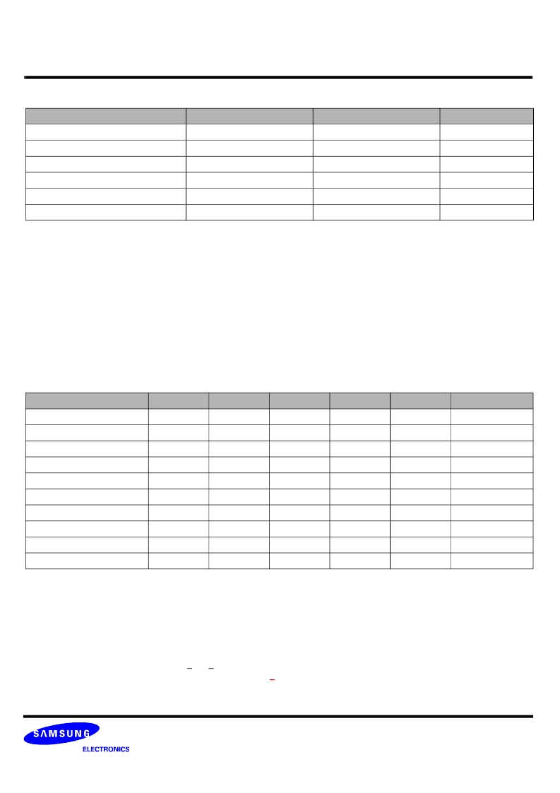
POWER & DC OPERATING CONDITIONS(SSTL_2 In/Out)
Recommended operating conditions(Voltage referenced to V
SS
=0V, T
A
=0 to 65
°
C)
Parameter
Symbol
Min
Typ
Max
Unit
Note
Device Supply voltage
V
DD
2.375
2.50
2.625
V
1,
7
Output Supply voltage
V
DDQ
2.375
2.50
2.625
V
1,
7
Reference voltage
V
REF
0.49*V
DDQ
-
0.51*V
DDQ
V
2
Termination voltage
Vtt
V
REF
-0.04
V
REF
V
REF
+0.04
V
3
Input logic high voltage
V
IH(DC)
V
REF
+0.15
-
V
DDQ
+0.30
V
4
Input logic low voltage
V
IL(DC)
-0.30
-
V
REF
-0.15
V
5
Output logic high voltage
V
OH
Vtt+0.76
-
-
V
I
OH
=-15.2mA
Output logic low voltage
V
OL
-
-
Vtt-0.76
V
I
OL
=+15.2mA
Input leakage current
I
IL
-5
-
5
uA
6
Output leakage current
I
OL
-5
-
5
uA
6
ABSOLUTE MAXIMUM RATINGS
Parameter
Symbol
Value
Unit
Voltage on any pin relative to Vss
V
IN
, V
OUT
-0.5 ~ 3.6
V
Voltage on V
DD
supply relative to Vss
V
DD
-1.0 ~ 3.6
V
Voltage on V
DD
supply relative to Vss
V
DDQ
-0.5 ~ 3.6
V
Storage temperature
T
STG
-55 ~ +150
°
C
Power dissipation
P
D
2.0
W
Short circuit current
I
OS
50
mA
1. Under all conditions V
DDQ
must be less than or equal to V
DD
.
2. V
REF
is expected to equal 0.50*V
DDQ
of the transmitting device and to track variations in the DC level of the same. Peak to
peak noise on the V
REF
may not exceed +
2% of the DC value. Thus, from 0.50*V
DDQ
, V
REF
is allowed +
25mV for DC error
and an additional +
25mV for AC noise.
3. V
tt
of the transmitting device must track V
REF
of the receiving device.
4. V
IH
(max.)= V
DDQ
+1.5V for a pulse width and it can not be greater than 1/3 of the cycle rate.
5. V
IL
(mim.)= -1.5V for a pulse width and it can not be greater than 1/3 of the cycle rate.
6. For any pin under test input of 0V < V
IN
< V
DD
is acceptable. For all other pins that are not under test V
IN
=0V.
7. For the K4D261638F-TC25/2A, VDD & VDDQ = 2.8V+0.1V
Note :
相關(guān)PDF資料 |
PDF描述 |
|---|---|
| K4D263238A | 1M x 32Bit x 4 Banks Double Data Rate Synchronous DRAM with Bi-directional Data Strobe and DLL |
| K4D263238A-GC33 | DIODE ZENER SINGLE 500mW 2.7Vz 0.05mA-Izt 0.05 1uA-Ir 1 SOD-123 3K/REEL |
| K4D263238A-GC36 | DIODE ZENER SINGLE 500mW 3Vz 0.05mA-Izt 0.05 0.8uA-Ir 1 SOD-123 3K/REEL |
| K4D263238A-GC40 | DIODE ZENER SINGLE 500mW 3.3Vz 0.05mA-Izt 0.05 7.5uA-Ir 1.5 SOD-123 3K/REEL |
| K4D263238A-GC45 | DIODE ZENER SINGLE 500mW 3.6Vz 0.05mA-Izt 0.05 7.5uA-Ir 2 SOD-123 3K/REEL |
相關(guān)代理商/技術(shù)參數(shù) |
參數(shù)描述 |
|---|---|
| K4D261638I-LC50000 | 制造商:Samsung Semiconductor 功能描述:DDR SGRAM X16 TSOP2 - Trays |
| K4D261638I-LC50T00 | 制造商:Samsung Semiconductor 功能描述:DDR SGRAM X16 TSOP2 - Tape and Reel |
| K4D261638K-LC50T00 | 制造商:Samsung Semiconductor 功能描述:128MSGDDRDDR SGRAMX16TSOP2 - Tape and Reel |
| K4D263238A | 制造商:SAMSUNG 制造商全稱:Samsung semiconductor 功能描述:1M x 32Bit x 4 Banks Double Data Rate Synchronous DRAM with Bi-directional Data Strobe and DLL |
| K4D263238A-GC33 | 制造商:SAMSUNG 制造商全稱:Samsung semiconductor 功能描述:1M x 32Bit x 4 Banks Double Data Rate Synchronous DRAM with Bi-directional Data Strobe and DLL |
發(fā)布緊急采購,3分鐘左右您將得到回復(fù)。