- 您現(xiàn)在的位置:買賣IC網(wǎng) > PDF目錄373060 > K4D551638D (SAMSUNG SEMICONDUCTOR CO. LTD.) 256Mbit GDDR SDRAM PDF資料下載
參數(shù)資料
| 型號: | K4D551638D |
| 廠商: | SAMSUNG SEMICONDUCTOR CO. LTD. |
| 英文描述: | 256Mbit GDDR SDRAM |
| 中文描述: | 片256Mbit GDDR SDRAM內(nèi)存 |
| 文件頁數(shù): | 11/18頁 |
| 文件大小: | 230K |
| 代理商: | K4D551638D |
256M GDDR SDRAM
K4D551638D-TC
- 11 -
Rev 1.8 (Oct. 2003)
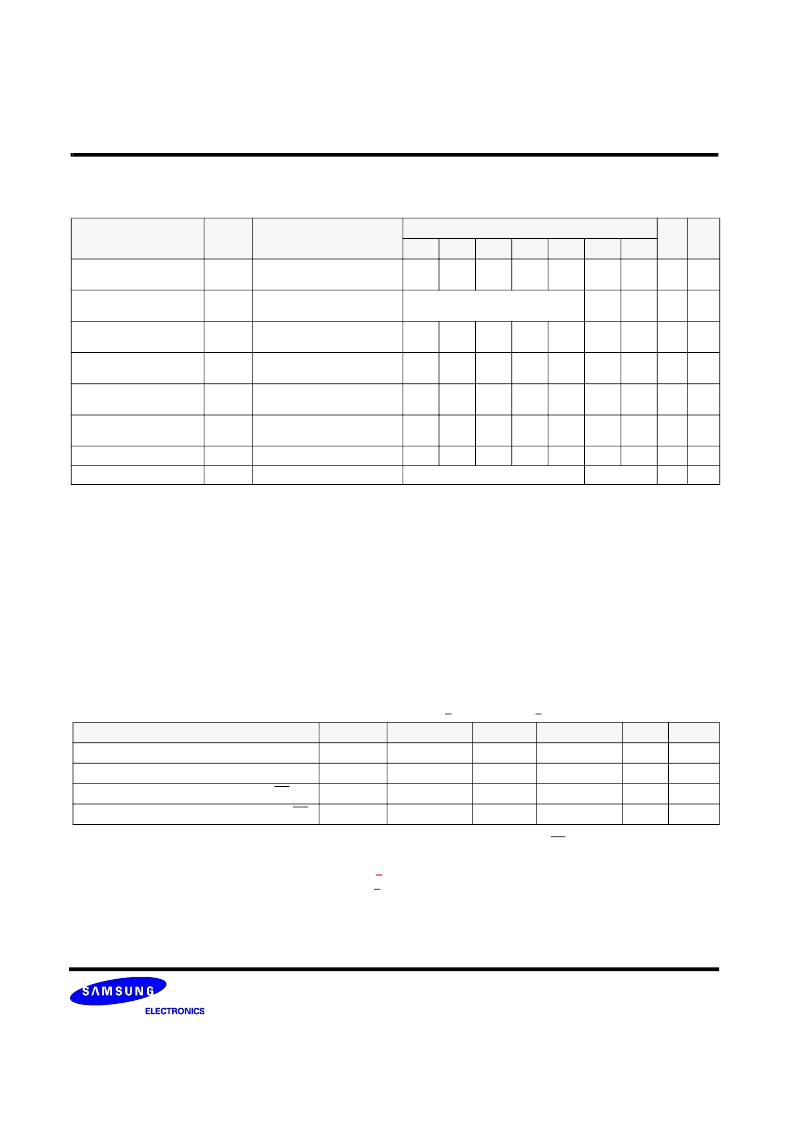
DC CHARACTERISTICS
Recommended operating conditions Unless Otherwise Noted, T
A
=0 to 65
°
C)
Note :
1. Measured with outputs open.
2. Refresh period is 32ms for -TC2A/33/36/40/45 (4K/32ms)
Refresh period is 64ms for -TC50/60 (8K/64ms)
Parameter
Symbol
Test Condition
Version
Unit Note
-2A
-33
-36
-40
-45
-50
-60
Operating Current
(One Bank Active)
ICC1
Burst Lenth=2 tRC
≥
tRC(min)
IOL=0mA, tCC= tCC(min)
TBD
230
220
210
200
145
125
mA
1
Precharge Standby Current
in Power-down mode
ICC2P
CKE
≤
VIL(max), tCC= tCC(min)
70
4
3
mA
Precharge Standby Current
in Non Power-down mode
ICC2N
CKE
≥
VIH(min), CS
≥
VIH(min),
tCC= tCC(min)
TBD
100
90
80
70
30
25
mA
Active Standby Current
power-down mode
ICC3P
CKE
≤
VIL(max), tCC= tCC(min)
TBD
80
75
70
65
55
35
mA
Active Standby Current in
in Non Power-down mode
ICC3N
CKE
≥
VIH(min), CS
≥
VIH(min),
tCC= tCC(min)
TBD
150
140
130
120
75
55
mA
Operating Current
( Burst Mode)
ICC4
tRC
≥
tRFC(min)tRC
≥
tRFC(min)
Page Burst, All Banks activated.
TBD
450
430
410
390
250
200
mA
Refresh Current
ICC5
tRC
≥
tRFC(min)
TBD
390
380
370
360
200
180
mA
2
Self Refresh Current
ICC6
CKE
≤
0.2V
4
3
mA
1. V
ID
is the magnitude of the difference between the input level on CK and the input level on CK
2. The value of V
IX
is expected to equal 0.5*V
DDQ
of the transmitting device and must track variations in the DC level of the same
3. For the K4D551638D-TC2A, VDD & VDDQ = 2.8V+0.1V.
4. For the K4D551638D-TC60, VDD & VDDQ = 2.5V+5%.
Note :
AC INPUT OPERATING CONDITIONS
Recommended operating conditions(Voltage referenced to V
SS
=0V, V
DD
=2.6V+
0.1V, V
DDQ
=2.6V+
0.1V ,T
A
=0 to 65
°
C)
Parameter
Symbol
Min
Typ
Max
Unit
Note
Input High (Logic 1) Voltage; DQ
V
IH
V
REF
+0.35
-
-
V
Input Low (Logic 0) Voltage; DQ
V
IL
-
-
V
REF
-0.35
V
Clock Input Differential Voltage; CK and CK
V
ID
0.7
-
V
DDQ
+0.6
V
1
Clock Input Crossing Point Voltage; CK and CK
V
IX
0.5*V
DDQ
-0.2
-
0.5*V
DDQ
+0.2
V
2
相關(guān)PDF資料 |
PDF描述 |
|---|---|
| K4D551638D-TC | 256Mbit GDDR SDRAM |
| K4D551638D-TC2A | 256Mbit GDDR SDRAM |
| K4D551638D-TC33 | 256Mbit GDDR SDRAM |
| K4D551638D-TC36 | 256Mbit GDDR SDRAM |
| K4D551638D-TC40 | 256Mbit GDDR SDRAM |
相關(guān)代理商/技術(shù)參數(shù) |
參數(shù)描述 |
|---|---|
| K4D551638D-TC | 制造商:SAMSUNG 制造商全稱:Samsung semiconductor 功能描述:256Mbit GDDR SDRAM |
| K4D551638D-TC2A | 制造商:SAMSUNG 制造商全稱:Samsung semiconductor 功能描述:256Mbit GDDR SDRAM |
| K4D551638D-TC33 | 制造商:SAMSUNG 制造商全稱:Samsung semiconductor 功能描述:256Mbit GDDR SDRAM |
| K4D551638D-TC36 | 制造商:SAMSUNG 制造商全稱:Samsung semiconductor 功能描述:256Mbit GDDR SDRAM |
| K4D551638D-TC40 | 制造商:SAMSUNG 制造商全稱:Samsung semiconductor 功能描述:256Mbit GDDR SDRAM |
發(fā)布緊急采購,3分鐘左右您將得到回復。