- 您現(xiàn)在的位置:買賣IC網(wǎng) > PDF目錄373062 > K4H560838E-ULA2 (SAMSUNG SEMICONDUCTOR CO. LTD.) 256Mb E-die DDR SDRAM Specification 66 TSOP-II with Pb-Free (RoHS compliant) PDF資料下載
參數(shù)資料
| 型號: | K4H560838E-ULA2 |
| 廠商: | SAMSUNG SEMICONDUCTOR CO. LTD. |
| 英文描述: | 256Mb E-die DDR SDRAM Specification 66 TSOP-II with Pb-Free (RoHS compliant) |
| 中文描述: | 256Mb的電子芯片與DDR SDRAM的規(guī)格鉛66 TSOP-II免費(符合RoHS) |
| 文件頁數(shù): | 7/19頁 |
| 文件大?。?/td> | 171K |
| 代理商: | K4H560838E-ULA2 |
DDR SDRAM
DDR SDRAM 256Mb F-die (x8, x16)
Rev. 1.1 August. 2003
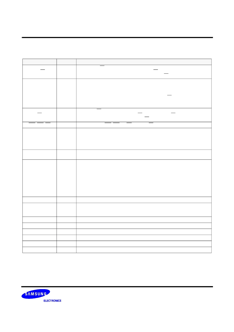
SYMBOL
TYPE
DESCRIPTION
CK, CK
Input
Clock : CK and CK are differential clock inputs. All address and control input signals are sam-
pled on the positive edge of CK and negative edge of CK. Output (read) data is referenced to
both edges of CK. Internal clock signals are derived from CK/CK.
CKE
Input
Clock Enable : CKE HIGH activates, and CKE LOW deactivates internal clock signals, and
device input buffers and output drivers. Deactivating the clock provides PRECHARGE
POWER-DOWN and SELF REFRESH operation (all banks idle), or ACTIVE POWER-DOWN
(row ACTIVE in any bank). CKE is synchronous for all functions except for disabling outputs,
which is achieved asynchronously. Input buffers, excluding CK, CK and CKE are disabled dur-
ing power-down and self refresh modes, providing low standby power. CKE will recognize an
LVCMOS LOW level prior to VREF being stable on power-up.
CS
Input
Chip Select : CS enables(registered LOW) and disables(registered HIGH) the command
decoder. All commands are masked when CS is registered HIGH. CS provides for external
bank selection on systems with multiple banks. CS is considered part of the command code.
RAS, CAS, WE
Input
Command Inputs : RAS, CAS and WE (along with CS) define the command being entered.
LDM,(UDM)
Input
Input Data Mask : DM is an input mask signal for write data. Input data is masked when DM is
sampled HIGH along with that input data during a WRITE access. DM is sampled on both
edges of DQS. Although DM pins are input only, the DM loading matches the DQ and DQS
loading. For the x16, LDM corresponds to the data on DQ0~D7 ; UDM corresponds to the data
on DQ8~DQ15. DM may be driven high, low, or floating during READs.
BA0, BA1
Input
Bank Addres Inputs : BA0 and BA1 define to which bank an ACTIVE, READ, WRITE or PRE-
CHARGE command is being applied.
A [0 : 12]
Input
Address Inputs : Provide the row address for ACTIVE commands, and the column address and
AUTO PRECHARGE bit for READ/WRITE commands, to select one location out of the mem-
ory array in the respective bank. A10 is sampled during a PRECHARGE command to deter-
mine whether the PRECHARGE applies to one bank (A10 LOW) or all banks (A10 HIGH). If
only one bank is to be precharged, the bank is selected by BA0, BA1. The address inputs also
provide the op-code during a MODE REGISTER SET command. BA0 and BA1 define which
mode register is loaded during the MODE REGISTER SET command (MRS or EMRS).
A12 & A13 are used on device densities of 256Mb and greater, and A13 is used only on 1Gb
decices.
DQ
I/O
Data Input/Output : Data bus
LDQS,(U)DQS
I/O
Data Strobe : Output with read data, input with write data. Edge-aligned with read data, cen-
tered in write data. Used to capture write data. For the x16, LDQS corresponds to the data on
DQ0~D7 ; UDQS corresponds to the data on DQ8~DQ15
NC
-
No Connect : No internal electrical connection is present.
VDDQ
Supply
DQ Power Supply : +2.6V
±
0.1V.
VSSQ
Supply
DQ Ground.
VDD
Supply
Power Supply : +2.6V
±
0.1V (device specific).
VSS
Supply
Ground.
VREF
Input
SSTL_2 reference voltage.
Input/Output Function Description
相關(guān)PDF資料 |
PDF描述 |
|---|---|
| K4H560838E-ULAA | 256Mb E-die DDR SDRAM Specification 66 TSOP-II with Pb-Free (RoHS compliant) |
| K4H560838E-VLB0 | 256Mb E-die DDR SDRAM Specification 54 sTSOP-II with Pb-Free (RoHS compliant) |
| K4H560838E-VLB3 | 256Mb E-die DDR SDRAM Specification 54 sTSOP-II with Pb-Free (RoHS compliant) |
| K4H560838F-UC | 256Mb F-die DDR400 SDRAM Specification |
| K4H560838A-TCA2 | Quad Micropower Precision Low-Voltage Operational Amplifier 14-SOIC |
相關(guān)代理商/技術(shù)參數(shù) |
參數(shù)描述 |
|---|---|
| K4H560838E-ULAA | 制造商:SAMSUNG 制造商全稱:Samsung semiconductor 功能描述:256Mb E-die DDR SDRAM Specification 66 TSOP-II with Pb-Free (RoHS compliant) |
| K4H560838E-ULB0 | 制造商:SAMSUNG 制造商全稱:Samsung semiconductor 功能描述:256Mb E-die DDR SDRAM Specification 66 TSOP-II with Pb-Free (RoHS compliant) |
| K4H560838E-ULB3 | 制造商:SAMSUNG 制造商全稱:Samsung semiconductor 功能描述:256Mb E-die DDR SDRAM Specification 66 TSOP-II with Pb-Free (RoHS compliant) |
| K4H560838E-VC/LA2 | 制造商:SAMSUNG 制造商全稱:Samsung semiconductor 功能描述:256Mb E-die DDR SDRAM Specification 54 sTSOP-II with Pb-Free (RoHS compliant) |
| K4H560838E-VC/LB0 | 制造商:SAMSUNG 制造商全稱:Samsung semiconductor 功能描述:256Mb E-die DDR SDRAM Specification 54 sTSOP-II with Pb-Free (RoHS compliant) |
發(fā)布緊急采購,3分鐘左右您將得到回復。