- 您現(xiàn)在的位置:買賣IC網(wǎng) > PDF目錄373080 > K7A803601M (SAMSUNG SEMICONDUCTOR CO. LTD.) 256Kx36 & 512Kx18 Synchronous SRAM PDF資料下載
參數(shù)資料
| 型號: | K7A803601M |
| 廠商: | SAMSUNG SEMICONDUCTOR CO. LTD. |
| 英文描述: | 256Kx36 & 512Kx18 Synchronous SRAM |
| 中文描述: | 256Kx36 |
| 文件頁數(shù): | 7/17頁 |
| 文件大小: | 466K |
| 代理商: | K7A803601M |
K7A801801M
256Kx36 & 512Kx18 Synchronous SRAM
- 7 -
Rev 3.0
May 1999
K7A803601M
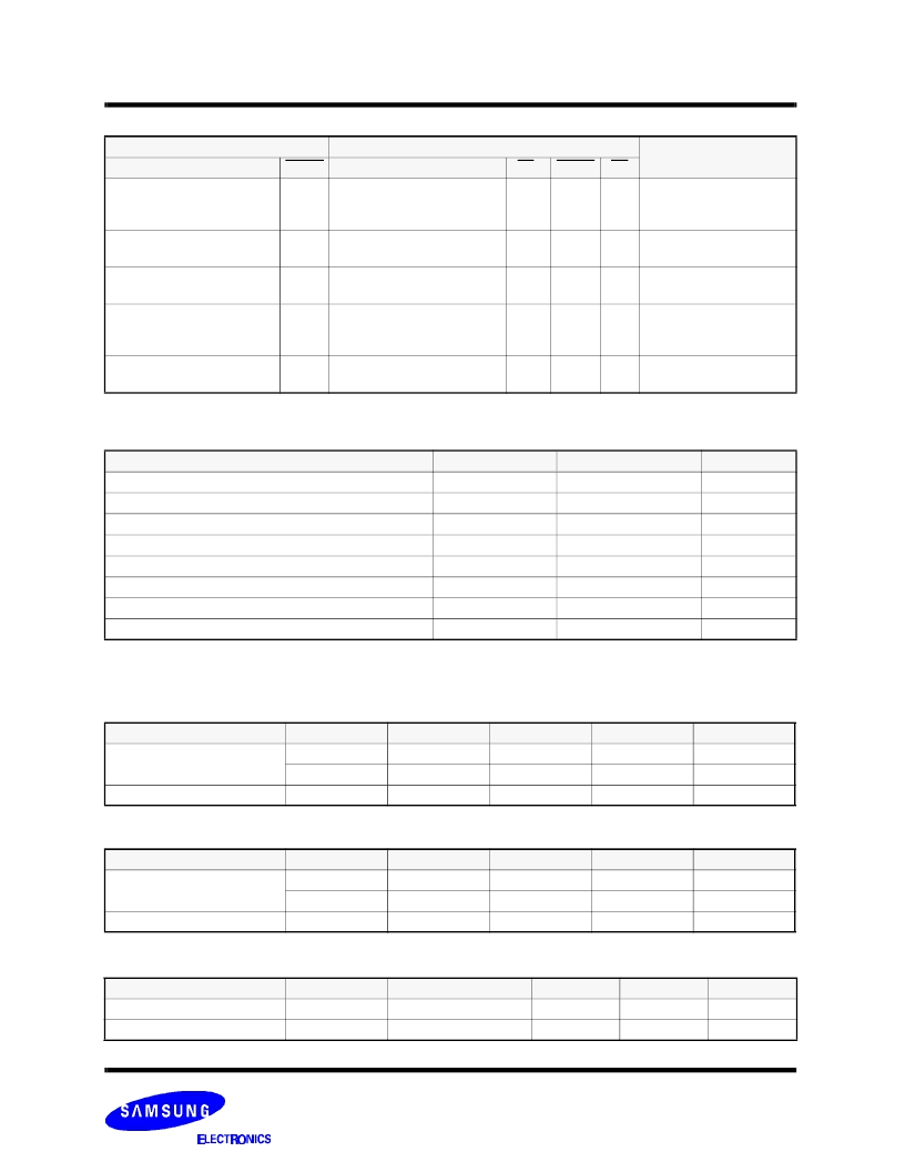
PASS-THROUGH TRUTH TABLE
Note :
1. This operation makes written data immediately available at output during a read cycle preceded by a write cycle.
PREVIOUS CYCLE
PRESENT CYCLE
NEXT CYCLE
OPERATION
WRITE
OPERATION
CS
1
WRITE
OE
Write Cycle, All bytes
Address=An-1, Data=Dn-1
All L
Initiate Read Cycle
Address=An
Data=Qn-1 for all bytes
L
H
L
Read Cycle
Data=Qn
Write Cycle, All bytes
Address=An-1, Data=Dn-1
All L
No new cycle
Data=Qn-1 for all bytes
H
H
L
No carryover from
previous cycle
Write Cycle, All bytes
Address=An-1, Data=Dn-1
All L
No new cycle
Data=High-Z
H
H
H
No carryover from
previous cycle
Write Cycle, One byte
Address=An-1, Data=Dn-1
One L
Initiate Read Cycle
Address=An
Data=Qn-1 for one byte
L
H
L
Read Cycle
Data=Qn
Write Cycle, One byte
Address=An-1, Data=Dn-1
One L
No new cycle
Data=Qn-1 for one byte
H
H
L
No carryover from
previous cycle
ABSOLUTE MAXIMUM RATINGS*
*Note :
Stresses greater than those listed under "Absolute Maximum Ratings" may cause permanent damage to the device. This is a stress rating only
and functional operation of the device at these or any other conditions above those indicated in the operating sections of this specification is not
implied. Exposure to absolute maximum rating conditions for extended periods may affect reliability.
PARAMETER
SYMBOL
RATING
UNIT
Voltage on V
DD
Supply Relative to V
SS
V
DD
-0.3 to 4.6
V
Voltage on V
DDQ
Supply Relative to V
SS
V
DDQ
V
DD
V
Voltage on Input Pin Relative to V
SS
V
IN
-0.3 to 4.6
V
Voltage on I/O Pin Relative to V
SS
V
IO
-0.3 to V
DDQ
+0.5
V
Power Dissipation
P
D
1.6
W
Storage Temperature
T
STG
-65 to 150
°
C
°
C
°
C
Operating Temperature
T
OPR
0 to 70
Storage Temperature Range Under Bias
T
BIAS
-10 to 85
CAPACITANCE*
(T
A
=25
°
C, f=1MHz)
*Note :
Sampled not 100% tested.
PARAMETER
SYMBOL
TEST CONDITION
MIN
MAX
UNIT
Input Capacitance
C
IN
V
IN
=0V
-
6
pF
Output Capacitance
C
OUT
V
OUT
=0V
-
8
pF
OPERATING CONDITIONS at 3.3V I/O
(0
°
C
≤
T
A
≤
70
°
C)
PARAMETER
SYMBOL
MIN
Typ.
MAX
UNIT
Supply Voltage
V
DD
3.135
3.3
3.465
V
V
DDQ
3.135
3.3
3.465
V
Ground
V
SS
0
0
0
V
OPERATING CONDITIONS at 2.5V I/O
(0
°
C
≤
T
A
≤
70
°
C)
PARAMETER
SYMBOL
MIN
Typ.
MAX
UNIT
Supply Voltage
V
DD
3.135
3.3
3.465
V
V
DDQ
2.375
2.5
2.9
V
Ground
V
SS
0
0
0
V
相關(guān)PDF資料 |
PDF描述 |
|---|---|
| K7A801809A | 256Kx36 & 512Kx18 Synchronous SRAM |
| K7A803609A | 256Kx36 & 512Kx18 Synchronous SRAM |
| K7A801809B | 256Kx36 & 512Kx18-Bit Synchronous Pipelined Burst SRAM |
| K7B803625 | 256Kx36 & 512Kx18-Bit Synchronous Pipelined Burst SRAM |
| K7B803625B-QC75 | 256Kx36 & 512Kx18-Bit Synchronous Pipelined Burst SRAM |
相關(guān)代理商/技術(shù)參數(shù) |
參數(shù)描述 |
|---|---|
| K7A803609A | 制造商:SAMSUNG 制造商全稱:Samsung semiconductor 功能描述:256Kx36 & 512Kx18 Synchronous SRAM |
| K7A803609B | 制造商:SAMSUNG 制造商全稱:Samsung semiconductor 功能描述:256Kx36 & 512Kx18-Bit Synchronous Pipelined Burst SRAM |
| K7A803609B_06 | 制造商:SAMSUNG 制造商全稱:Samsung semiconductor 功能描述:256Kx36 & 512Kx18 Synchronous SRAM |
| K7A803609B-PI25000 | 制造商:Samsung SDI 功能描述: |
| K7A803609B-QC25 | 制造商:SAMSUNG 制造商全稱:Samsung semiconductor 功能描述:256Kx36 & 512Kx18-Bit Synchronous Pipelined Burst SRAM |
發(fā)布緊急采購,3分鐘左右您將得到回復(fù)。