- 您現(xiàn)在的位置:買賣IC網(wǎng) > PDF目錄373080 > K7B801825B-QC75 (SAMSUNG SEMICONDUCTOR CO. LTD.) 256Kx36 & 512Kx18-Bit Synchronous Pipelined Burst SRAM PDF資料下載
參數(shù)資料
| 型號(hào): | K7B801825B-QC75 |
| 廠商: | SAMSUNG SEMICONDUCTOR CO. LTD. |
| 英文描述: | 256Kx36 & 512Kx18-Bit Synchronous Pipelined Burst SRAM |
| 中文描述: | 256Kx36 |
| 文件頁(yè)數(shù): | 3/18頁(yè) |
| 文件大小: | 400K |
| 代理商: | K7B801825B-QC75 |
第1頁(yè)第2頁(yè)當(dāng)前第3頁(yè)第4頁(yè)第5頁(yè)第6頁(yè)第7頁(yè)第8頁(yè)第9頁(yè)第10頁(yè)第11頁(yè)第12頁(yè)第13頁(yè)第14頁(yè)第15頁(yè)第16頁(yè)第17頁(yè)第18頁(yè)
K7A801809B
256Kx36 & 512Kx18 Synchronous SRAM
- 3 -
Rev 3.0
Nov. 2003
K7A803609B
256Kx36 & 512Kx18-bit Synchronous Pipelined Burst SRAM
The K7A803609B and K7A801809B are 9,437,184-bit Syn-
chronous Static Random Access Memory designed for high
performance second level cache of Pentium and Power PC
based System.
It is organized as 256K(512K) words of 36(18) bits and inte-
grates address and control registers, a 2-bit burst address
counter and added some new functions for high perfor-
mance cache RAM applications; GW, BW, LBO, ZZ. Write
cycles are internally self-timed and synchronous.
Full bus-width write is done by GW, and each byte write is
performed by the combination of WEx and BW when GW is
high. And with CS
1
high, ADSP is blocked to control signals.
Burst cycle can be initiated with either the address status
processor(ADSP) or address status cache controller(ADSC)
inputs. Subsequent burst addresses are generated inter-
nally in the system
′
s burst sequence and are controlled by
the burst address advance(ADV) input.
LBO pin is DC operated and determines burst sequence(lin-
ear or interleaved).
ZZ pin controls Power Down State and reduces Stand-by
current regardless of CLK.
The K7A803609B and K7A801809B are fabricated using
SAMSUNG
′
s high performance CMOS technology and is
available in a 100pin TQFP and Multiple power and ground
pins are utilized to minimize ground bounce.
GENERAL DESCRIPTION
FEATURES
Synchronous Operation.
2 Stage Pipelined operation with 4 Burst.
On-Chip Address Counter.
Self-Timed Write Cycle.
On-Chip Address and Control Registers.
3.3V+0.165V/-0.165V Power Supply.
I/O Supply Voltage 3.3V+0.165V/-0.165V for 3.3V I/O
or 2.5V+0.4V/-0.125V for 2.5V I/O
5V Tolerant Inputs Except I/O Pins.
Byte Writable Function.
Global Write Enable Controls a full bus-width write.
Power Down State via ZZ Signal.
LBO Pin allows a choice of either a interleaved burst or a linear
burst.
Three Chip Enables for simple depth expansion with No Data
Contention only for TQFP ; 2cycle Enable, 1cycle Disable.
Asynchronous Output Enable Control.
ADSP, ADSC, ADV Burst Control Pins.
TTL-Level Three-State Output.
100-TQFP-1420A
Operating in commeical and industrial temperature range.
FAST ACCESS TIMES
PARAMETER
Symbol
-25
Unit
Cycle Time
tCYC
4.0
ns
Clock Access Time
tCD
2.6
ns
Output Enable Access Time
tOE
2.6
ns
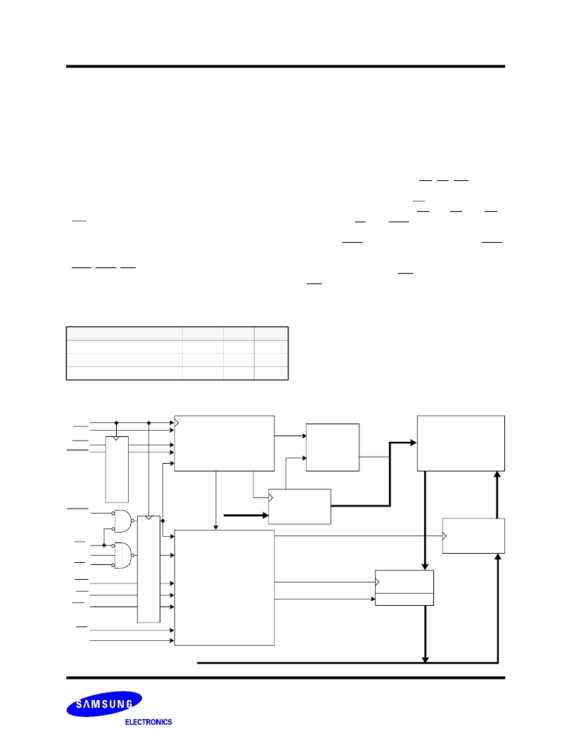
LOGIC BLOCK DIAGRAM
CLK
LBO
ADV
ADSC
ADSP
CS
1
CS
2
CS
2
GW
BW
WEx
(x=a,b,c,d or a,b)
OE
ZZ
DQa0 ~ DQd7 or DQa0 ~ DQb7
DQPa ~ DQPd
a
,DQP
b
BURST CONTROL
LOGIC
BURST
ADDRESS
COUNTER
256Kx36 , 512Kx18
MEMORY
ARRAY
ADDRESS
REGISTER
CONTROL
LOGIC
OUTPUT
REGISTER
DATA-IN
REGISTER
BUFFER
C
R
C
R
A
′
0
~A
′
1
A
0
~A
1
or A
2
~A
18
or A
0
~A
18
A
0
~A
17
A
2
~A
17
相關(guān)PDF資料 |
PDF描述 |
|---|---|
| K7B803625B-QC65 | 256Kx36 & 512Kx18-Bit Synchronous Pipelined Burst SRAM |
| K7B161825A | Aluminum Snap-In Capacitor; Capacitance: 470uF; Voltage: 250V; Case Size: 25x30 mm; Packaging: Bulk |
| K7B163625A | Aluminum Snap-In Capacitor; Capacitance: 820uF; Voltage: 250V; Case Size: 25x40 mm; Packaging: Bulk |
| K7A161800A | Aluminum Snap-In Capacitor; Capacitance: 330uF; Voltage: 400V; Case Size: 35x25 mm; Packaging: Bulk |
| K7A161801A | Aluminum Snap-In Capacitor; Capacitance: 330uF; Voltage: 400V; Case Size: 22x50 mm; Packaging: Bulk |
相關(guān)代理商/技術(shù)參數(shù) |
參數(shù)描述 |
|---|---|
| K7B801825B-QC75000 | 制造商:Samsung Semiconductor 功能描述:SRAM Chip Sync Dual 3.3V 9M-Bit 512K x 18 7.5ns 100-Pin TQFP Tray |
| K7B801825M | 制造商:SAMSUNG 制造商全稱:Samsung semiconductor 功能描述:256Kx36 & 512Kx18 Synchronous SRAM |
| K7B803625 | 制造商:SAMSUNG 制造商全稱:Samsung semiconductor 功能描述:256Kx36 & 512Kx18-Bit Synchronous Pipelined Burst SRAM |
| K7B803625B | 制造商:SAMSUNG 制造商全稱:Samsung semiconductor 功能描述:256Kx36 & 512Kx18 Synchronous SRAM |
| K7B803625B-PC65T00 | 制造商:Samsung Semiconductor 功能描述: |
發(fā)布緊急采購(gòu),3分鐘左右您將得到回復(fù)。