- 您現(xiàn)在的位置:買賣IC網(wǎng) > PDF目錄373086 > K9F1208D0B (SAMSUNG SEMICONDUCTOR CO. LTD.) Circular Connector; MIL SPEC:MIL-DTL-38999 Series III; Body Material:Metal; Series:TV07; No. of Contacts:128; Connector Shell Size:25; Connecting Termination:Crimp; Circular Shell Style:Jam Nut Receptacle; Body Style:Straight PDF資料下載
參數(shù)資料
| 型號(hào): | K9F1208D0B |
| 廠商: | SAMSUNG SEMICONDUCTOR CO. LTD. |
| 元件分類: | 圓形連接器 |
| 英文描述: | Circular Connector; MIL SPEC:MIL-DTL-38999 Series III; Body Material:Metal; Series:TV07; No. of Contacts:128; Connector Shell Size:25; Connecting Termination:Crimp; Circular Shell Style:Jam Nut Receptacle; Body Style:Straight |
| 中文描述: | 6400 × 8位NAND閃存 |
| 文件頁數(shù): | 36/45頁 |
| 文件大?。?/td> | 767K |
| 代理商: | K9F1208D0B |
第1頁第2頁第3頁第4頁第5頁第6頁第7頁第8頁第9頁第10頁第11頁第12頁第13頁第14頁第15頁第16頁第17頁第18頁第19頁第20頁第21頁第22頁第23頁第24頁第25頁第26頁第27頁第28頁第29頁第30頁第31頁第32頁第33頁第34頁第35頁當(dāng)前第36頁第37頁第38頁第39頁第40頁第41頁第42頁第43頁第44頁第45頁
FLASH MEMORY
36
K9F1208U0B
K9F1208D0B
Advance
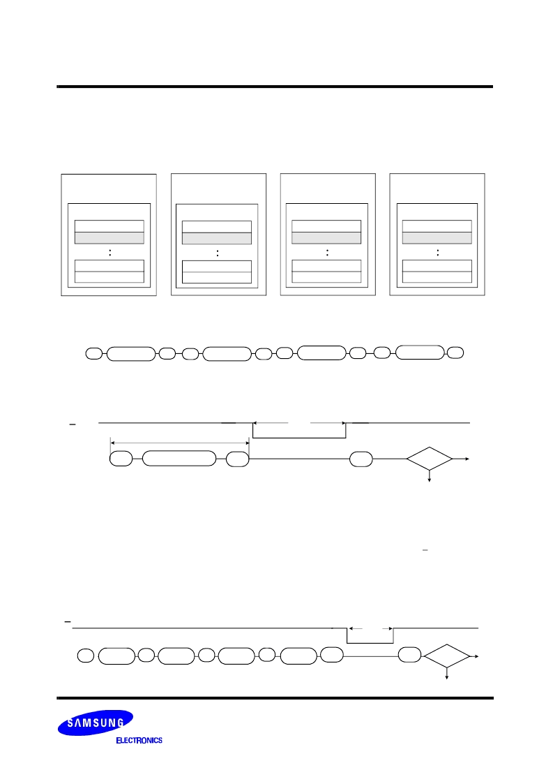
Restriction in addressing with Multi Plane Page Program
While any block in each plane may be addressable for Multi-Plane Page Program, the five least significant addresses(A9-A13) for the
selected pages at one operation must be the same. Figure 14 shows an example where 2nd page of each addressed block is
selected for four planes. However, any arbitrary sequence is allowed in addressing multiple planes as shown in Figure15.
80h
Plane 2
11h
80h
11h
80h
11h
80h
10h
Plane 0
Plane3
Plane 1
Plane 0
(1024 Block)
Plane 1
(1024 Block)
Plane 2
(1024 Block)
Plane 3
(1024 Block)
Page 0
Page 1
Page 31
Page 30
Block 0
Page 0
Page 1
Page 31
Page 30
Block 1
Page 0
Page 1
Page 31
Page 30
Block 2
Page 0
Page 1
Page 31
Page 30
Block 3
Figure 16. Multi-Plane Page Program & Read Status Operation
80h
9
~ A
25
528 bytes
I/O
0
~
7
R/B
Address & Data Input
I/O
Pass
10h
71h
Fail
t
PROG
Last Plane input
Multi-Plane Block Erase
Basic concept of Multi-Plane Block Erase operation is identical to that of Multi-Plane Page Program. Up to four blocks, one from each
plane can be simultaneously erased. Standard Block Erase command sequences (Block Erase Setup command followed by three
address cycles) may be repeated up to four times for erasing up to four blocks. Only one block should be selected from each plane.
The Erase Confirm command initiates the actual erasing process. The completion is detected by analyzing R/B pin or Ready/Busy
status (I/O 6). Upon the erase completion, pass/fail status of each block is examined by reading extended pass/fail status(I/O 1
through I/O 4).
Figure 17. Four Block Erase Operation
60h
A
0
~ A
7
& A
9
~ A
25
I/O
X
R/B
Address
(3 Cycle)
60h
60h
60h
D0h
71h
I/O
Pass
Fail
t
BERS
Address
(3 Cycle)
Address
(3 Cycle)
Address
(3 Cycle)
Figure 14. Multi-Plane Program & Read Status Operation
Figure 15. Addressing Multiple Planes
相關(guān)PDF資料 |
PDF描述 |
|---|---|
| K9F1208D0B-D | TV 128C 128#22D SKT RECP |
| K9F1208D0B-Y | 64M x 8 Bit NAND Flash Memory |
| K9F1208U0B-D | 64M x 8 Bit NAND Flash Memory |
| K9F1208U0B-V | 64M x 8 Bit NAND Flash Memory |
| K9F1208U0B-Y | 64M x 8 Bit NAND Flash Memory |
相關(guān)代理商/技術(shù)參數(shù) |
參數(shù)描述 |
|---|---|
| K9F1208D0B-D | 制造商:SAMSUNG 制造商全稱:Samsung semiconductor 功能描述:64M x 8 Bit NAND Flash Memory |
| K9F1208D0B-Y | 制造商:SAMSUNG 制造商全稱:Samsung semiconductor 功能描述:64M x 8 Bit NAND Flash Memory |
| K9F1208Q0A | 制造商:SAMSUNG 制造商全稱:Samsung semiconductor 功能描述:512Mb/256Mb 1.8V NAND Flash Errata |
| K9F1208Q0A-XXB0 | 制造商:SAMSUNG 制造商全稱:Samsung semiconductor 功能描述:512Mb/256Mb 1.8V NAND Flash Errata |
| K9F1208Q0B | 制造商:SAMSUNG 制造商全稱:Samsung semiconductor 功能描述:64M x 8 Bit NAND Flash Memory |
發(fā)布緊急采購,3分鐘左右您將得到回復(fù)。