- 您現(xiàn)在的位置:買賣IC網(wǎng) > PDF目錄373129 > KFG2816D1M-DIB (SAMSUNG SEMICONDUCTOR CO. LTD.) OneNAND SPECIFICATION PDF資料下載
參數(shù)資料
| 型號: | KFG2816D1M-DIB |
| 廠商: | SAMSUNG SEMICONDUCTOR CO. LTD. |
| 英文描述: | OneNAND SPECIFICATION |
| 中文描述: | OneNAND的規(guī)格 |
| 文件頁數(shù): | 31/87頁 |
| 文件大?。?/td> | 1175K |
| 代理商: | KFG2816D1M-DIB |
第1頁第2頁第3頁第4頁第5頁第6頁第7頁第8頁第9頁第10頁第11頁第12頁第13頁第14頁第15頁第16頁第17頁第18頁第19頁第20頁第21頁第22頁第23頁第24頁第25頁第26頁第27頁第28頁第29頁第30頁當(dāng)前第31頁第32頁第33頁第34頁第35頁第36頁第37頁第38頁第39頁第40頁第41頁第42頁第43頁第44頁第45頁第46頁第47頁第48頁第49頁第50頁第51頁第52頁第53頁第54頁第55頁第56頁第57頁第58頁第59頁第60頁第61頁第62頁第63頁第64頁第65頁第66頁第67頁第68頁第69頁第70頁第71頁第72頁第73頁第74頁第75頁第76頁第77頁第78頁第79頁第80頁第81頁第82頁第83頁第84頁第85頁第86頁第87頁
OneNAND128
FLASH MEMORY
31
8. Device Operation
The device supports both a limited command based and a register based interface for performing operations on the device, reading
device ID, writing data to buffer etc. The command based interface is active in the boot partition, i.e. commands can only be written
with a boot area address. Boot area data is only returned if no command has been issued prior to the read.
8.1 Command based operation
The entire address range, except for the boot area, can be used for the data buffer. All commands are written to the boot partition. Writes outside the
boot partition are treated as normal writes to the buffers or registers. The command consists of one or more cycles depending on the command. After
completion of the command the device starts its execution. Writing incorrect information which include address and data or writing an improper command
will terminate the previous command sequence and make the device go to the ready status. The defined valid command sequences are stated in Table4.
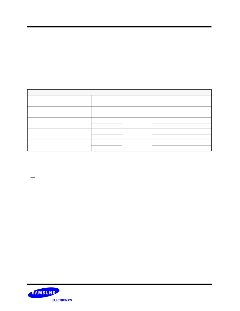
Table 4. Command Sequences
NOTE:
1) DP(Data Partition) : DataRAM Area
2) BP(Boot Partition) : BootRAM Area [0000h ~ 01FFh, 8000h ~ 800Fh].
3) Load Data into Buffer operation is available within a block(64KB)
4) Load 1KB unit into DataRAM0. Current Start address(FPA) is automatically incremented by 1KB unit after the load.
5) 0000h -> Data is Manufacturer ID
0001h -> Data is Device ID
0002h -> Current Block Write Protection Status
6) WE toggling can terminate ’Read Identification Data’ operation.
8.1.1 Read Data from Buffer
Buffer can be read by addressing a read to a wanted buffer area
8.1.2 Write Data to Buffer
Buffer can be written by addressing a write to a wanted buffer area
8.1.3 Reset OneNAND
Reset command is given by writing 00F0h to the boot partition address. Reset will return all default values into the device.
8.1.4 Load Data into Buffer
Load Data into Buffer command is a two-cycle command. Two sequential designated command activates this operation. Sequentially writing 00E0h
and 0000h to the boot partition [0000h~01FFh, 8000h~800Fh] will load one page to DataRAM0. This operation refers to FBA and FPA. FSA, BSA, and
BSC are not considered.
At the end of this operation, FPA will be automatically increased by 1. So continuous issue of this command will sequentially load data in next page to
DataRAM0. This page address increment is restricted within a block.
The default value of FBA and FPA is 0. Therefore, initial issue of this command after power on will load the first page of memory, which is usually boot
code.
8.1.5 Read Identification Data
Read Identification Data command consists of two cycles. It gives out the devices identification data according to the given address. The first cycle is
0090h to the boot partition address and second cycle is read from the addresses specified in Table5.
Command Definition
Cycles
1st cycle
2nd cycle
Read Data from Buffer
Add
1
DP
1)
Data
Data
Write Data to Buffer
Add
1
DP
Data
Data
Reset OneNAND
Add
1
BP
2)
Data
00F0h
Load Data into Buffer
3)
Add
2
BP
BP
Data
00E0h
0000h
4)
Read Identification Data
6)
Add
2
BP
XXXXh
5)
Data
0090h
Data
相關(guān)PDF資料 |
PDF描述 |
|---|---|
| KFG2816D1M-DID | OneNAND SPECIFICATION |
| KFG2816D1M-PEB | OneNAND SPECIFICATION |
| KFG2816D1M-PED | OneNAND SPECIFICATION |
| KFG2816D1M-PIB | OneNAND SPECIFICATION |
| KFH1G16D2M-DEB | FLASH MEMORY |
相關(guān)代理商/技術(shù)參數(shù) |
參數(shù)描述 |
|---|---|
| KFG2816D1M-DID | 制造商:SAMSUNG 制造商全稱:Samsung semiconductor 功能描述:OneNAND SPECIFICATION |
| KFG2816D1M-PEB | 制造商:SAMSUNG 制造商全稱:Samsung semiconductor 功能描述:OneNAND SPECIFICATION |
| KFG2816D1M-PED | 制造商:SAMSUNG 制造商全稱:Samsung semiconductor 功能描述:OneNAND SPECIFICATION |
| KFG2816D1M-PIB | 制造商:SAMSUNG 制造商全稱:Samsung semiconductor 功能描述:OneNAND SPECIFICATION |
| KFG2816D1M-PID | 制造商:SAMSUNG 制造商全稱:Samsung semiconductor 功能描述:OneNAND SPECIFICATION |
發(fā)布緊急采購,3分鐘左右您將得到回復(fù)。