- 您現(xiàn)在的位置:買(mǎi)賣(mài)IC網(wǎng) > PDF目錄373127 > KFH2G16U2M-DID6 (SAMSUNG SEMICONDUCTOR CO. LTD.) FLASH MEMORY(54MHz) PDF資料下載
參數(shù)資料
| 型號(hào): | KFH2G16U2M-DID6 |
| 廠商: | SAMSUNG SEMICONDUCTOR CO. LTD. |
| 英文描述: | FLASH MEMORY(54MHz) |
| 中文描述: | 閃存(54MHz之間) |
| 文件頁(yè)數(shù): | 73/125頁(yè) |
| 文件大小: | 1657K |
| 代理商: | KFH2G16U2M-DID6 |
第1頁(yè)第2頁(yè)第3頁(yè)第4頁(yè)第5頁(yè)第6頁(yè)第7頁(yè)第8頁(yè)第9頁(yè)第10頁(yè)第11頁(yè)第12頁(yè)第13頁(yè)第14頁(yè)第15頁(yè)第16頁(yè)第17頁(yè)第18頁(yè)第19頁(yè)第20頁(yè)第21頁(yè)第22頁(yè)第23頁(yè)第24頁(yè)第25頁(yè)第26頁(yè)第27頁(yè)第28頁(yè)第29頁(yè)第30頁(yè)第31頁(yè)第32頁(yè)第33頁(yè)第34頁(yè)第35頁(yè)第36頁(yè)第37頁(yè)第38頁(yè)第39頁(yè)第40頁(yè)第41頁(yè)第42頁(yè)第43頁(yè)第44頁(yè)第45頁(yè)第46頁(yè)第47頁(yè)第48頁(yè)第49頁(yè)第50頁(yè)第51頁(yè)第52頁(yè)第53頁(yè)第54頁(yè)第55頁(yè)第56頁(yè)第57頁(yè)第58頁(yè)第59頁(yè)第60頁(yè)第61頁(yè)第62頁(yè)第63頁(yè)第64頁(yè)第65頁(yè)第66頁(yè)第67頁(yè)第68頁(yè)第69頁(yè)第70頁(yè)第71頁(yè)第72頁(yè)當(dāng)前第73頁(yè)第74頁(yè)第75頁(yè)第76頁(yè)第77頁(yè)第78頁(yè)第79頁(yè)第80頁(yè)第81頁(yè)第82頁(yè)第83頁(yè)第84頁(yè)第85頁(yè)第86頁(yè)第87頁(yè)第88頁(yè)第89頁(yè)第90頁(yè)第91頁(yè)第92頁(yè)第93頁(yè)第94頁(yè)第95頁(yè)第96頁(yè)第97頁(yè)第98頁(yè)第99頁(yè)第100頁(yè)第101頁(yè)第102頁(yè)第103頁(yè)第104頁(yè)第105頁(yè)第106頁(yè)第107頁(yè)第108頁(yè)第109頁(yè)第110頁(yè)第111頁(yè)第112頁(yè)第113頁(yè)第114頁(yè)第115頁(yè)第116頁(yè)第117頁(yè)第118頁(yè)第119頁(yè)第120頁(yè)第121頁(yè)第122頁(yè)第123頁(yè)第124頁(yè)第125頁(yè)
OneNAND1G(KFG1G16Q2M-DEB5)
FLASH MEMORY
73
OneNAND2G(KFH2G16Q2M-DEB5)
OneNAND4G(KFW4G16Q2M-DEB5)
The device is designed to offer protection from any involuntary program/erase during power-transitions.
An internal voltage detector disables all functions whenever Vcc is below POR level, about 1.3V. It is recommended that the RP pin,
which provides hardware protection, should be kept at VIL before power-down.
3.6 Load Operation
See Timing Diagram 6.8
The Load operation is initiated by setting up the start address from which the data is to be loaded. The Load command is issued in
order to initiate the load.
During a Load operation, the device:
-Transfers the data from NAND Flash array into the BufferRAM
-ECC is checked and any detected and corrected error is reported in the status response as well as
any unrecoverable error.
Once the BufferRAM has been filled, an interrupt is issued to the host so that the contents of the BufferRAM can be read. The read
from the BufferRAM can be an asynchronous read mode or synchronous read mode. The status information related to load operation
can be checked by the host if required.
The device has a dual data buffer memory architecture (DataRAM0, DataRAM1), each 2KB in size. Each DataRAM buffer has 4
Sectors. The device is capable of independent and simultaneous data-read operation from one data buffer and data-load operation to
the other data buffer. Refer to the information for more details in section 3.12.1, "Read-While-Load Operation".
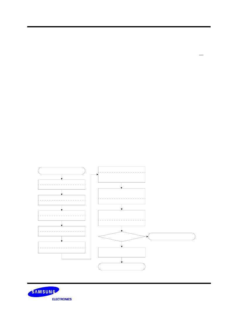
Load Operation Flow Chart Diagram
Start
Write ’DFS*, FBA’ of Flash
Add: F100h DQ=FBA
Write ’FPA, FSA’ of Flash
Add: F107h DQ=FPA, FSA
Write ’BSA, BSC’ of DataRAM
Add: F200h DQ=BSA, BSC
Select DataRAM for DDP
Add: F101h DQ=DBS
Write ’Load’ Command
Add: F220h
DQ=0000h or 0013h
Wait for INT register
low to high transition
Add: F241h DQ[15]=INT
Read Controller
Status Register
Add: F240h DQ[10]=Error
DQ[10]=0
NO
YES
* DBS, DFS is for DDP
Host reads data from
DataRAM
Read completed
Map Out
Write 0 to interrupt register
Add: F241h DQ=0000h
3.5 Data Protection During Power Down Operation
See Timing Diagram 6.15
相關(guān)PDF資料 |
PDF描述 |
|---|---|
| KFH4G1612M-DEB5 | FLASH MEMORY(54MHz) |
| KFH4G1612M-DED5 | FLASH MEMORY(54MHz) |
| KFH4G16D2M-DEB5 | FLASH MEMORY(54MHz) |
| KFH4G16D2M-DEB6 | FLASH MEMORY(54MHz) |
| KFH4G16D2M-DED5 | FLASH MEMORY(54MHz) |
相關(guān)代理商/技術(shù)參數(shù) |
參數(shù)描述 |
|---|---|
| KFH-440-10 | 制造商:PennEngineering (PEM) 功能描述: |
| KFH-440-12ET | 制造商:PennEngineering (PEM) 功能描述: |
| KFH4405 | 制造商:n/a 功能描述:Ships in 2 days |
| KFH-440-5ET | 制造商:PennEngineering (PEM) 功能描述: |
| KFH4406 | 制造商:n/a 功能描述:Ships in 2 days |
發(fā)布緊急采購(gòu),3分鐘左右您將得到回復(fù)。