- 您現(xiàn)在的位置:買賣IC網 > PDF目錄373157 > KM416L8031BT-G(L)Z (SAMSUNG SEMICONDUCTOR CO. LTD.) DDR SDRAM Specification Version 1.0 PDF資料下載
參數資料
| 型號: | KM416L8031BT-G(L)Z |
| 廠商: | SAMSUNG SEMICONDUCTOR CO. LTD. |
| 英文描述: | DDR SDRAM Specification Version 1.0 |
| 中文描述: | DDR SDRAM的規(guī)范版本1.0 |
| 文件頁數: | 19/53頁 |
| 文件大小: | 669K |
| 代理商: | KM416L8031BT-G(L)Z |
第1頁第2頁第3頁第4頁第5頁第6頁第7頁第8頁第9頁第10頁第11頁第12頁第13頁第14頁第15頁第16頁第17頁第18頁當前第19頁第20頁第21頁第22頁第23頁第24頁第25頁第26頁第27頁第28頁第29頁第30頁第31頁第32頁第33頁第34頁第35頁第36頁第37頁第38頁第39頁第40頁第41頁第42頁第43頁第44頁第45頁第46頁第47頁第48頁第49頁第50頁第51頁第52頁第53頁
- 19 -
REV. 1.0 November. 2. 2000
128Mb DDR SDRAM
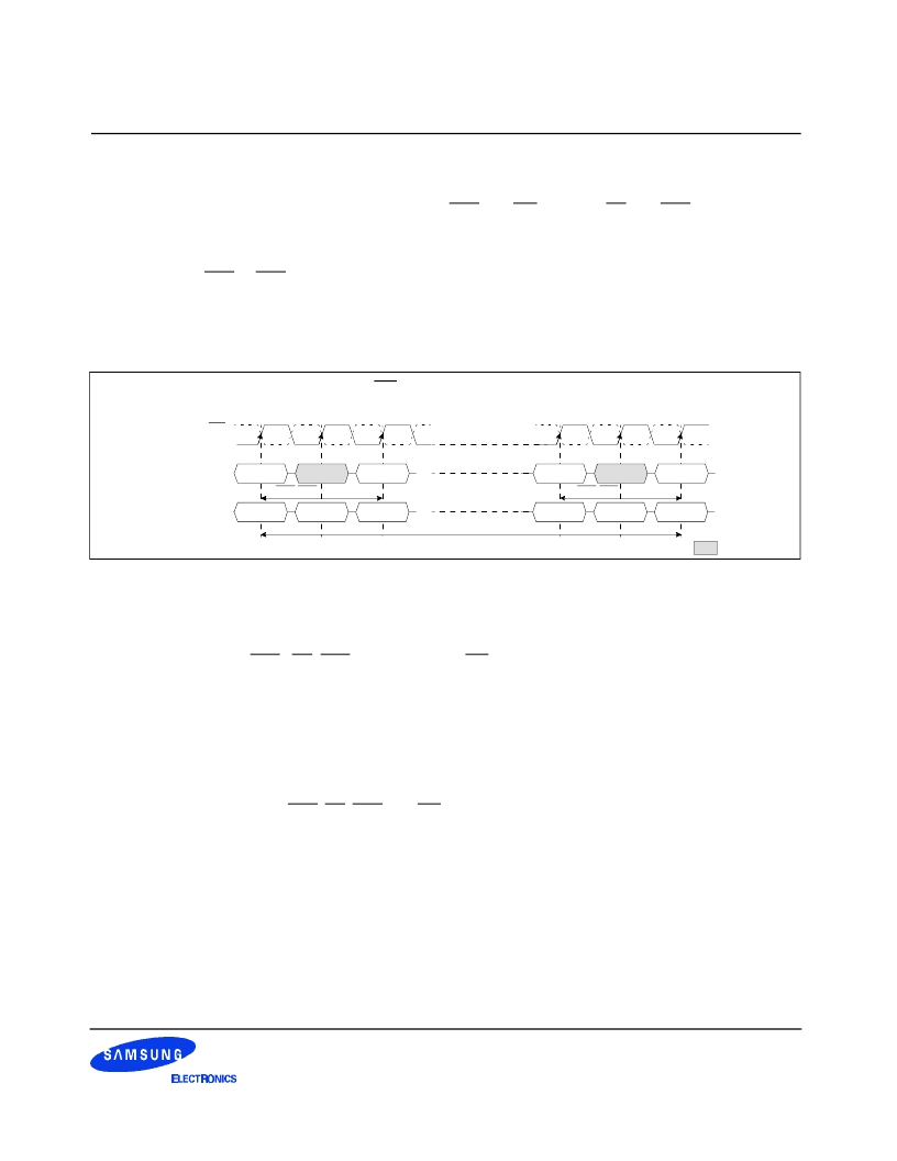
3.2.5 Row Active
The Bank Activation command is issued by holding CAS and WE high with CS and RAS low at the rising
edge of the clock(CK). The DDR SDRAM has four independent banks, so two Bank Select addresses(BA0,
BA1) are required. The Bank Activation command must be applied before any Read or Write operation is exe-
cuted. The delay from the Bank Activation command to the first read or write command must meet or exceed
the minimum of RAS to CAS delay time(tRCD min). Once a bank has been activated, it must be precharged
before another Bank Activation command can be applied to the same bank. The minimum time interval
between interleaved Bank Activation commands(Bank A to Bank B and vice versa) is the Bank to Bank delay
time(tRRD min).
Address
Command
RAS-CAS delay(
t
RCD
)
Bank A
Bank Activation Command Cycle
(CAS Latency = 2)
Bank A
Row Addr.
Bank A
Col. Addr.
Write A
Precharge
NOP
RAS-RAS delay time(
t
RRD
)
Bank B
Row Addr.
Bank A
Row. Addr.
Bank B
Bank A
NOP
ROW Cycle Time(
t
RC
)
Tn
Tn+1
Tn+2
2
0
1
: Don
′
t care
CK
CK
3.2.6 Read Bank
3.2.7 Write Bank
This command is used after the row activate command to initiate the burst read of data. The read command
is initiated by activating RAS, CS, CAS, and deasserting WE at the same clock sampling(rising) edge as
described in the command truth table. The length of the burst and the CAS latency time will be determined by
the values programmed during the MRS command.
This command is used after the row activate command to initiate the burst write of data. The write com-
mand is initiated by activating RAS, CS, CAS, and WE at the same clock sampling(rising) edge as described in
the command truth table. The length of the burst will be determined by the values programmed during the
MRS command.
Figure 8. Bank activation command cycle timing
相關PDF資料 |
PDF描述 |
|---|---|
| KM44L32031BT-G(F)0 | DDR SDRAM Specification Version 0.61 |
| KM48L16031BT-G(F)0 | DDR SDRAM Specification Version 0.61 |
| KM416L8031BT-G(F)0 | DDR SDRAM Specification Version 0.61 |
| KM44L32031BT-G(F)Y | DDR SDRAM Specification Version 0.61 |
| KM48L16031BT-G(F)Y | DDR SDRAM Specification Version 0.61 |
相關代理商/技術參數 |
參數描述 |
|---|---|
| KM416L8031BT-GLZ/Y/0 | 制造商:SAMSUNG 制造商全稱:Samsung semiconductor 功能描述:DDR SDRAM Specification Version 1.0 |
| KM416RD16AC | 制造商:SAMSUNG 制造商全稱:Samsung semiconductor 功能描述:128/144Mbit RDRAM 256K x 16/18 bit x 2*16 Dependent Banks Direct RDRAMTM |
| KM416RD16AD | 制造商:SAMSUNG 制造商全稱:Samsung semiconductor 功能描述:128/144Mbit RDRAM 256K x 16/18 bit x 2*16 Dependent Banks Direct RDRAMTM |
| KM416RD16C | 制造商:SAMSUNG 制造商全稱:Samsung semiconductor 功能描述:128/144Mbit RDRAM 256K x 16/18 bit x 2*16 Dependent Banks Direct RDRAMTM |
| KM416RD16D | 制造商:SAMSUNG 制造商全稱:Samsung semiconductor 功能描述:128/144Mbit RDRAM 256K x 16/18 bit x 2*16 Dependent Banks Direct RDRAMTM |
發(fā)布緊急采購,3分鐘左右您將得到回復。