- 您現(xiàn)在的位置:買賣IC網(wǎng) > PDF目錄3952 > KMPC8358EVRAGDDA (Freescale Semiconductor)IC MPU POWERQUICC II PRO 668PBGA PDF資料下載
參數(shù)資料
| 型號(hào): | KMPC8358EVRAGDDA |
| 廠商: | Freescale Semiconductor |
| 文件頁數(shù): | 75/95頁 |
| 文件大小: | 0K |
| 描述: | IC MPU POWERQUICC II PRO 668PBGA |
| 標(biāo)準(zhǔn)包裝: | 2 |
| 系列: | MPC83xx |
| 處理器類型: | 32-位 MPC83xx PowerQUICC II Pro |
| 速度: | 400MHz |
| 電壓: | 1.2V |
| 安裝類型: | 表面貼裝 |
| 封裝/外殼: | 668-BBGA 裸露焊盤 |
| 供應(yīng)商設(shè)備封裝: | 668-PBGA-PGE(29x29) |
| 包裝: | 托盤 |
第1頁第2頁第3頁第4頁第5頁第6頁第7頁第8頁第9頁第10頁第11頁第12頁第13頁第14頁第15頁第16頁第17頁第18頁第19頁第20頁第21頁第22頁第23頁第24頁第25頁第26頁第27頁第28頁第29頁第30頁第31頁第32頁第33頁第34頁第35頁第36頁第37頁第38頁第39頁第40頁第41頁第42頁第43頁第44頁第45頁第46頁第47頁第48頁第49頁第50頁第51頁第52頁第53頁第54頁第55頁第56頁第57頁第58頁第59頁第60頁第61頁第62頁第63頁第64頁第65頁第66頁第67頁第68頁第69頁第70頁第71頁第72頁第73頁第74頁當(dāng)前第75頁第76頁第77頁第78頁第79頁第80頁第81頁第82頁第83頁第84頁第85頁第86頁第87頁第88頁第89頁第90頁第91頁第92頁第93頁第94頁第95頁
MPC8358E PowerQUICC II Pro Processor Revision 2.1 PBGA Silicon Hardware Specifications, Rev. 3
Freescale Semiconductor
77
Clocking
The system VCO frequency is derived from the following equations:
csb_clk = {PCI_SYNC_IN × (1 + CFG_CLKIN_DIV)} × SPMF
System VCO Frequency = csb_clk × VCO divider (if both RCWL[DDRCM] and RCWL[LBCM]
are cleared)
OR
System VCO frequency = 2
× csb_clk × VCO divider (if either RCWL[DDRCM] or
RCWL[LBCM] are set).
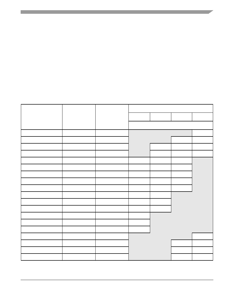
As described in Section 22, “Clocking,” the LBCM, DDRCM, and SPMF parameters in the reset
configuration word low and the CFG_CLKIN_DIV configuration input signal select the ratio between the
primary clock input (CLKIN or PCI_CLK) and the internal coherent system bus clock (csb_clk). Table 70
shows the expected frequency values for the CSB frequency for select csb_clk to CLKIN/PCI_SYNC_IN
ratios.
Table 70. CSB Frequency Options
CFG_CLKIN_DIV
at Reset1
SPMF
csb_clk:
Input Clock Ratio2
Input Clock Frequency (MHz)2
16.67
25
33.33
66.67
csb_clk Frequency (MHz)
Low
0010
2:1
133
Low
0011
3:1
100
200
Low
0100
4:1
100
133
266
Low
0101
5:1
125
166
333
Low
0110
6:1
100
150
200
Low
0111
7:1
116
175
233
Low
1000
8:1
133
200
266
Low
1001
9:1
150
225
300
Low
1010
10:1
166
250
333
Low
1011
11:1
183
275
Low
1100
12:1
200
300
Low
1101
13:1
216
325
Low
1110
14:1
233
Low
1111
15:1
250
Low
0000
16:1
266
High
0010
2:1
133
High
0011
3:1
100
200
High
0100
4:1
133
266
High
0101
5:1
166
333
相關(guān)PDF資料 |
PDF描述 |
|---|---|
| 84533-6 | CONN FFC 6POS 1.25MM R/A PCB |
| KMPC8358CZQAGDDA | IC MPU POWERQUICC II PRO 668PBGA |
| 84534-6 | CONN FFC 6POS 1.25MM VERT PCB |
| KMPC8358CVRAGDDA | IC MPU POWERQUICC II PRO 668PBGA |
| 395-010-521-801 | CARD EDGE 10POS DL .100X.200 BLK |
相關(guān)代理商/技術(shù)參數(shù) |
參數(shù)描述 |
|---|---|
| KMPC8358EVRAGDGA | 功能描述:微處理器 - MPU 8358 PBGA ENCRP NO-PB RoHS:否 制造商:Atmel 處理器系列:SAMA5D31 核心:ARM Cortex A5 數(shù)據(jù)總線寬度:32 bit 最大時(shí)鐘頻率:536 MHz 程序存儲(chǔ)器大小:32 KB 數(shù)據(jù) RAM 大小:128 KB 接口類型:CAN, Ethernet, LIN, SPI,TWI, UART, USB 工作電源電壓:1.8 V to 3.3 V 最大工作溫度:+ 85 C 安裝風(fēng)格:SMD/SMT 封裝 / 箱體:FBGA-324 |
| KMPC8358EVVAGDG | 功能描述:微處理器 - MPU 8360 TBGA ENCRP NOPB RoHS:否 制造商:Atmel 處理器系列:SAMA5D31 核心:ARM Cortex A5 數(shù)據(jù)總線寬度:32 bit 最大時(shí)鐘頻率:536 MHz 程序存儲(chǔ)器大小:32 KB 數(shù)據(jù) RAM 大小:128 KB 接口類型:CAN, Ethernet, LIN, SPI,TWI, UART, USB 工作電源電壓:1.8 V to 3.3 V 最大工作溫度:+ 85 C 安裝風(fēng)格:SMD/SMT 封裝 / 箱體:FBGA-324 |
| KMPC8358EVVAGDGA | 功能描述:微處理器 - MPU 8360 TBGA ENCRP NO-PB RoHS:否 制造商:Atmel 處理器系列:SAMA5D31 核心:ARM Cortex A5 數(shù)據(jù)總線寬度:32 bit 最大時(shí)鐘頻率:536 MHz 程序存儲(chǔ)器大小:32 KB 數(shù)據(jù) RAM 大小:128 KB 接口類型:CAN, Ethernet, LIN, SPI,TWI, UART, USB 工作電源電壓:1.8 V to 3.3 V 最大工作溫度:+ 85 C 安裝風(fēng)格:SMD/SMT 封裝 / 箱體:FBGA-324 |
| KMPC8358EZQAGDDA | 功能描述:微處理器 - MPU 8358 PBGA ENCRP RoHS:否 制造商:Atmel 處理器系列:SAMA5D31 核心:ARM Cortex A5 數(shù)據(jù)總線寬度:32 bit 最大時(shí)鐘頻率:536 MHz 程序存儲(chǔ)器大小:32 KB 數(shù)據(jù) RAM 大小:128 KB 接口類型:CAN, Ethernet, LIN, SPI,TWI, UART, USB 工作電源電壓:1.8 V to 3.3 V 最大工作溫度:+ 85 C 安裝風(fēng)格:SMD/SMT 封裝 / 箱體:FBGA-324 |
| KMPC8358EZQAGDGA | 功能描述:微處理器 - MPU 8358 PBGA ENCRP RoHS:否 制造商:Atmel 處理器系列:SAMA5D31 核心:ARM Cortex A5 數(shù)據(jù)總線寬度:32 bit 最大時(shí)鐘頻率:536 MHz 程序存儲(chǔ)器大小:32 KB 數(shù)據(jù) RAM 大小:128 KB 接口類型:CAN, Ethernet, LIN, SPI,TWI, UART, USB 工作電源電壓:1.8 V to 3.3 V 最大工作溫度:+ 85 C 安裝風(fēng)格:SMD/SMT 封裝 / 箱體:FBGA-324 |
發(fā)布緊急采購,3分鐘左右您將得到回復(fù)。