- 您現(xiàn)在的位置:買賣IC網(wǎng) > PDF目錄377592 > L29C520PC22 (LOGIC DEVICES INC) Pipeline Register PDF資料下載
參數(shù)資料
| 型號: | L29C520PC22 |
| 廠商: | LOGIC DEVICES INC |
| 元件分類: | 數(shù)字信號處理外設(shè) |
| 英文描述: | Pipeline Register |
| 中文描述: | 8-BIT, DSP-PIPELINE REGISTER, PDIP24 |
| 封裝: | 0.300 INCH, PLASTIC, DIP-24 |
| 文件頁數(shù): | 1/8頁 |
| 文件大小: | 188K |
| 代理商: | L29C520PC22 |
DEVICES INCORPORATED
L29C520/521
4 x 8-bit Multilevel Pipeline Register
4 x 8-bit Multilevel Pipeline Register
Pipeline Registers
08/02/2000–LDS.520/1-P
1
K
Four 8-bit Registers
K
Implements Double 2-Stage Pipeline
or Single 4-Stage Pipeline Register
K
Hold, Shift, and Load Instructions
K
Separate Data In and Data Out Pins
K
High-Speed, Low Power CMOS
Technology
K
Three-State Outputs
K
Replaces IDT29FCT520/IDT29FCT521
and AMD Am29520/Am29521
K
Package Styles Available:
24-pin PDIP
28-pin PLCC, J-Lead
FEATURES
DESCRIPTION
DEVICES INCORPORATED
The
L29C520
and
L29C521
are pin-
for-pin compatible with the
IDT29FCT520/IDT29FCT521 and
AMD Am29520/Am29521, imple-
mented in low power CMOS.
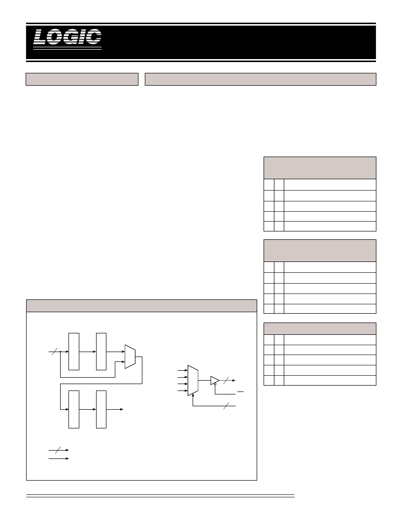
The L29C520 and L29C521 contain
four registers which can be configured
as two independent, 2-level pipelines
or as one 4-level pipeline.
The Instruction pins, I
1-0
, control the
loading of the registers. For either
device, the registers may be config-
ured as a four-stage delay line, with
data loaded into R1 and shifted
sequentially through R2, R3, and R4.
Also, for the L29C520, data may be
loaded from the inputs into either R1
or R3 with only R2 or R4 shifting. The
L29C521 differs from the L29C520 in
that R2 and R4 remain unchanged
during this type of data load, as
shown in Tables 1 and 2. Finally, I
1-0
may be set to prevent any register
from changing.
The S
1-0
select lines control a 4-to-1
multiplexer which routes the contents
of any of the registers to the Y output
pins. The independence of the I and S
controls allows simultaneous write
and read operations on different
registers.
S
1
S
0
Register Selected
L
L
Register 4
L
H
Register 3
H
L
Register 2
H
H
Register 1
T
ABLE
3.
O
UTPUT
S
ELECT
I
1
I
0
Description
L
L
D
R1
R1
R2
R2
R3
R3
R4
L
H
HOLD
HOLD
D
R3
HOLD
H
L
D
R1
HOLD
HOLD
HOLD
H
H
ALL REGISTERS ON HOLD
T
ABLE
2.
L29C521 I
NSTRUCTION
T
ABLE
I
1
I
0
Description
L
L
D
R1
R1
R2
R2
R3
R3
R4
L
H
HOLD
HOLD
D
R3
R3
R4
H
L
D
R1
R1
R2
HOLD
HOLD
H
H
ALL REGISTERS ON HOLD
T
ABLE
1.
L29C520 I
NSTRUCTION
T
ABLE
L29C520/521 B
LOCK
D
IAGRAM
M
REG 1
REG 2
REG 3
REG 4
R
R
R
R
M
D
8-0
8
8
OE
Y
7-0
S
1-0
I
1-0
CLK
2
2
相關(guān)PDF資料 |
PDF描述 |
|---|---|
| L29C525 | Dual Pipeline Register |
| L29C525JC15 | Dual Pipeline Register |
| L29C525JC20 | Dual Pipeline Register |
| L2N3904 | General Purpose Transistors NPN Silicon |
| L2N5401 | Amplifier Transistors PNP Silicon |
相關(guān)代理商/技術(shù)參數(shù) |
參數(shù)描述 |
|---|---|
| L29C520PC-22 | 制造商:LOGIC 功能描述: |
| L29C520PC25 | 制造商:未知廠家 制造商全稱:未知廠家 功能描述:Pipeline Register |
| L29C520SC14 | 制造商:未知廠家 制造商全稱:未知廠家 功能描述:Pipeline Register |
| L29C520SC22 | 制造商:未知廠家 制造商全稱:未知廠家 功能描述:Pipeline Register |
| L29C521CC14 | 制造商:未知廠家 制造商全稱:未知廠家 功能描述:Pipeline Register |
發(fā)布緊急采購,3分鐘左右您將得到回復(fù)。