- 您現(xiàn)在的位置:買賣IC網(wǎng) > PDF目錄69003 > L6229QTR (STMICROELECTRONICS) BRUSHLESS DC MOTOR CONTROLLER, 2.8 A, QCC32 PDF資料下載
參數(shù)資料
| 型號: | L6229QTR |
| 廠商: | STMICROELECTRONICS |
| 元件分類: | 運動控制電子 |
| 英文描述: | BRUSHLESS DC MOTOR CONTROLLER, 2.8 A, QCC32 |
| 封裝: | 5 X 5 MM, 1 MM HEIGHT, 0.50 MM PITCH, ROHS COMPLIANT, VFQFPN-32 |
| 文件頁數(shù): | 13/28頁 |
| 文件大小: | 521K |
| 代理商: | L6229QTR |
第1頁第2頁第3頁第4頁第5頁第6頁第7頁第8頁第9頁第10頁第11頁第12頁當(dāng)前第13頁第14頁第15頁第16頁第17頁第18頁第19頁第20頁第21頁第22頁第23頁第24頁第25頁第26頁第27頁第28頁

Circuit description
L6229Q
20/28
Doc ID 15209 Rev 3
5.7
Non-dissipative overcurrent detection and protection
The L6229Q integrates an overcurrent detection circuit (OCD) for full protection. This circuit
provides output-to-output and output-to-ground short circuit protection as well. With this
internal over current detection, the external current sense resistor normally used and its
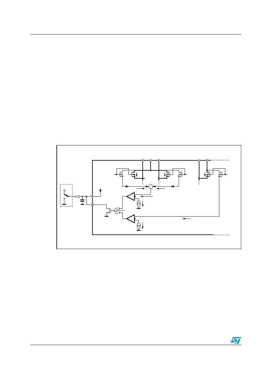
associated power dissipation are eliminated. Figure 19 shows a simplified schematic for the
overcurrent detection circuit.
To implement the over current detection, a sensing element that delivers a small but precise
fraction of the output current is implemented with each high side power MOS. Since this
current is a small fraction of the output current there is very little additional power
dissipation. This current is compared with an internal reference current IREF. When the
output current reaches the detection threshold (typically ISOVER = 2.8 A) the OCD
comparator signals a fault condition. When a fault condition is detected, an internal open
drain MOS with a pull down capability of 4 mA connected to pin DIAG is turned on.
The pin DIAG can be used to signal the fault condition to a
μC or to shut down the three-
phase bridge simply by connecting it to pin EN and adding an external R-C (see REN, CEN).
Figure 19.
Overcurrent protection simplified schematic
recovering normal operation can be easily programmed by means of the accurate
thresholds of the logic inputs. It is affected whether by CEN and REN values and its
an overcurrent has been detected depends only by CEN value. Its magnitude is reported in
CEN is also used for providing immunity to pin EN against fast transient noises. Therefore
the value of CEN should be chosen as big as possible according to the maximum tolerable
delay time and the REN value should be chosen according to the desired disable time.
The resistor REN should be chosen in the range from 2.2 kΩ to 180 kΩ. Recommended
values for REN and CEN are respectively 100 kΩ and 5.6 nF that allow obtaining 200 μs
disable time.
+
OVER TEMPERATURE
IREF
I1+I2 / n
I1 / n
HIGH SIDE DMOS
POWER SENSE
1 cell
POWER SENSE
1 cell
POWER SENSE
1 cell
POWER DMOS
n cells
POWER DMOS
n cells
POWER DMOS
n cells
HIGH SIDE DMOS
OUT1
OUT2
VSA
OUT3
VSB
I1
I2
I3
I2/ n
I3/ n
OCD
COMPARATOR
TO GATE
LOGIC
INTERNAL
OPEN-DRAIN
RDS(ON)
40
Ω TYP.
CEN
REN
DIAG
EN
VDD
μC or LOGIC
D02IN1381
相關(guān)PDF資料 |
PDF描述 |
|---|---|
| L6229Q | BRUSHLESS DC MOTOR CONTROLLER, 2.8 A, QCC32 |
| L6230PDTR | BRUSHLESS DC MOTOR CONTROLLER, 2.8 A, PDSO36 |
| L6230PD | BRUSHLESS DC MOTOR CONTROLLER, 2.8 A, PDSO36 |
| L6260 | DISK DRIVE MOTOR CONTROLLER, 1.5 A, PQFP64 |
| L6561I | 0.7 A POWER FACTOR CONTROLLER, PDIP8 |
相關(guān)代理商/技術(shù)參數(shù) |
參數(shù)描述 |
|---|---|
| L622C | 制造商:未知廠家 制造商全稱:未知廠家 功能描述:THYRISTOR MODULE|BRIDGE|HALF-CNTLD|CA|240V V(RRM)|46A I(T) |
| L622-DBC | 制造商:未知廠家 制造商全稱:未知廠家 功能描述:L series PRTDs, type L 622 DBC are designed for large volume applications where longterm stability |
| L622DY | 制造商:VCC 功能描述:LED CIRCUIT BOARD INDICATOR |
| L622F | 功能描述:分立半導(dǎo)體模塊 SCR/DIODE MODULE 240VAC 42.5ADC 600VP RoHS:否 制造商:Infineon Technologies 產(chǎn)品:Thyristor Power Modules 類型:Phase Controls 安裝風(fēng)格:Screw 封裝 / 箱體:DT61 封裝: |
| L622F-8680 | 制造商:Crydom 功能描述: |
發(fā)布緊急采購,3分鐘左右您將得到回復(fù)。