- 您現(xiàn)在的位置:買賣IC網(wǎng) > PDF目錄43900 > L6599N (STMICROELECTRONICS) 0.8 A SWITCHING CONTROLLER, 500 kHz SWITCHING FREQ-MAX, PDIP16 PDF資料下載
參數(shù)資料
| 型號: | L6599N |
| 廠商: | STMICROELECTRONICS |
| 元件分類: | 穩(wěn)壓器 |
| 英文描述: | 0.8 A SWITCHING CONTROLLER, 500 kHz SWITCHING FREQ-MAX, PDIP16 |
| 封裝: | LEAD FREE, PLASTIC, DIP-16 |
| 文件頁數(shù): | 22/36頁 |
| 文件大?。?/td> | 636K |
| 代理商: | L6599N |
第1頁第2頁第3頁第4頁第5頁第6頁第7頁第8頁第9頁第10頁第11頁第12頁第13頁第14頁第15頁第16頁第17頁第18頁第19頁第20頁第21頁當(dāng)前第22頁第23頁第24頁第25頁第26頁第27頁第28頁第29頁第30頁第31頁第32頁第33頁第34頁第35頁第36頁

L6599
Application information
29/36
voltage on the pin exceeds 7 V the device is shutdown. If its supply voltage is always above
the UVLO threshold, the IC will restart as the voltage falls below 7 V.
The LINE pin, while the device is operating, is a high impedance input connected to high
value resistors, thus it is prone to pick up noise, which might alter the OFF threshold or give
origin to undesired switch-off of the IC during ESD tests. It is possible to bypass the pin to
ground with a small film capacitor (e.g. 1-10 nF) to prevent any malfunctioning of this kind. If
the function is not used the pin has to be connected to a voltage greater than 1.25 V but
lower than 6V (worst-case value of the 7 V threshold).
7.7
Bootstrap section
The supply of the floating high-side section is obtained by means of a bootstrap circuitry.
This solution normally requires a high voltage fast recovery diode to charge the bootstrap
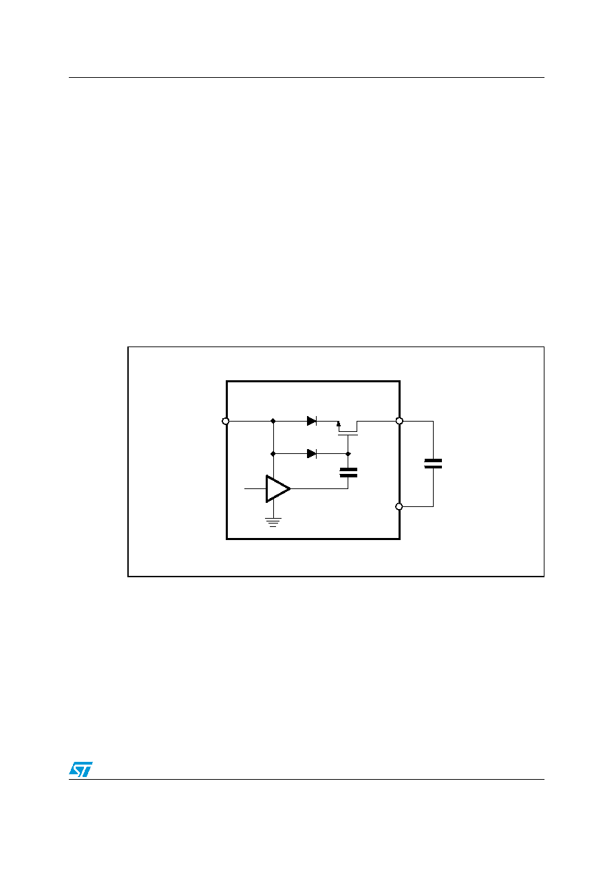
capacitor CBOOT. In the L6599 a patented integrated structure, replaces this external diode.
It is realized by means of a high voltage DMOS, working in the third quadrant and driven
synchronously with the low side driver (LVG), with a diode in series to the source, as shown
in Figure 34.
Figure 34. Bootstrap supply: internal bootstrap synchronous diode
The diode prevents any current can flow from the VBOOT pin back to VCC in case that the
supply is quickly turned off when the internal capacitor of the pump is not fully discharged.
To drive the synchronous DMOS it is necessary a voltage higher than the supply voltage
The bootstrap structure introduces a voltage drop while recharging CBOOT (i.e. when the low
side driver is on), which increases with the operating frequency and with the size of the
external power MOSFET. It is the sum of the drop across the RDS(on) and the forward drop
across the series diode. At low frequency this drop is very small and can be neglected but,
as the operating frequency increases, it must be taken into account. In fact, the drop
reduces the amplitude of the driving signal and can significantly increase the RDS(on) of the
external high-side MOSFET and then its conductive loss.
L6599
14
OUT
16
VBOOT
Vcc
12
LVG
CBOOT
相關(guān)PDF資料 |
PDF描述 |
|---|---|
| L6599TR | 0.8 A SWITCHING CONTROLLER, 500 kHz SWITCHING FREQ-MAX, PDSO16 |
| L6610D | 6-CHANNEL POWER SUPPLY SUPPORT CKT, PDSO24 |
| L6610N | 6-CHANNEL POWER SUPPLY SUPPORT CKT, PDIP24 |
| L6611DTRT | POWER SUPPLY SUPPORT CKT, PDSO20 |
| L6611D | 5-CHANNEL POWER SUPPLY SUPPORT CKT, PDSO20 |
相關(guān)代理商/技術(shù)參數(shù) |
參數(shù)描述 |
|---|---|
| L6599NR | 功能描述:電壓模式 PWM 控制器 HV resonant CNTRL RoHS:否 制造商:Texas Instruments 輸出端數(shù)量:1 拓撲結(jié)構(gòu):Buck 輸出電壓:34 V 輸出電流: 開關(guān)頻率: 工作電源電壓:4.5 V to 5.5 V 電源電流:600 uA 最大工作溫度:+ 125 C 最小工作溫度:- 40 C 封裝 / 箱體:WSON-8 封裝:Reel |
| L6599TR | 制造商:STMICROELECTRONICS 制造商全稱:STMicroelectronics 功能描述:High-voltage resonant controller |
| L65B | 制造商:Electro-Mech 功能描述: |
| L65B3C881-00000-000 | 制造商:Carling Technologies 功能描述:L-SERIES ROCKER SWITCH - Bulk |
| L65D1CNN1-00000-000 | 制造商:Carling Technologies 功能描述:L-SERIES ROCKER SWITCH - Bulk |
發(fā)布緊急采購,3分鐘左右您將得到回復(fù)。