- 您現(xiàn)在的位置:買賣IC網(wǎng) > PDF目錄30731 > LC72720Y (SANYO SEMICONDUCTOR CO LTD) SPECIALTY CONSUMER CIRCUIT, PDIP24 PDF資料下載
參數(shù)資料
| 型號: | LC72720Y |
| 廠商: | SANYO SEMICONDUCTOR CO LTD |
| 元件分類: | 消費家電 |
| 英文描述: | SPECIALTY CONSUMER CIRCUIT, PDIP24 |
| 封裝: | SDIP-24 |
| 文件頁數(shù): | 12/14頁 |
| 文件大小: | 107K |
| 代理商: | LC72720Y |

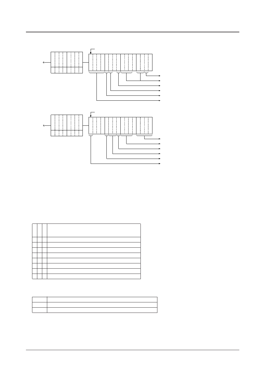
CCB Input Data Format
Caution: The bits labeled with an asterisk must be set to 0.
(1) Synchronization protection (forward protection) method setting (4 bits): FS0 to FS3
FS3 = 0: If offset words in the correct order could not be detected continuously during the number of blocks specified
by FS0 to FS2, take that to be a lost synchronization state.
FS3 = 1: If blocks with uncorrectable errors were received consecutively during the number of blocks specified by
FS0 to FS2, take that to be a lost synchronization state.
No. 6488-7/14
LC72720Y, 72720YV
Initial value: FS0 = 0, FS1 = 1, FS2 = 0, FS3 = 0
Initial value: BS = 0
FFF
S
Condition for detecting lost synchronization
012
0
If 3 consecutive blocks matching the FS3 condition are received.
1
0
If 4 consecutive blocks matching the FS3 condition are received.
0
1
0
If 5 consecutive blocks matching the FS3 condition are received.
1
0
If 6 consecutive blocks matching the FS3 condition are received.
0
1
If 8 consecutive blocks matching the FS3 condition are received.
1
0
1
If 10 consecutive blocks matching the FS3 condition are received.
0
1
If 12 consecutive blocks matching the FS3 condition are received.
1
If 16 consecutive blocks matching the FS3 condition are received.
(2) Synchronization detection method setting (1 bit): BS
BS
Synchronization detection conditions
0
If during 3 blocks, 2 blocks of offset words were detected in the correct order.
1
If the offset words were detected in the correct order in 2 consecutive blocks.
DI
A13208
0
B0
1
B1
0
B2
1
B3
0
A0
1
A1
1
A2
0
A3
FS0FS1FS2FS3 BS SYR
*
** *
*
**
OWEEC0 EC1 EC2
EC3 EC4 CT0
DI
A13209
1
B0
1
B1
0
B2
1
B3
0
A0
1
A1
1
A2
0
A3
CT1
XS PL0 PL1 RM PT0 PT1 PT2
TS0 TS1 TS2 TS3
[1] CCB address 6A
[2] CCB address 6B
IN1 data, first bit
IN2 data, first bit
(11) Circuit control
(5) Error correction method setting
(4) RAM write control
(3) Synchronization and RAM address reset
(2) Synchronization detection method setting
(1) Synchronization protection method setting
(10) Test mode settings
(9) Output pin settings
(8) RDS/RBDS selection
(7) Demodulation circuit phase control
(6) Crystal oscillator frequency selection
(11) Circuit control
相關(guān)PDF資料 |
PDF描述 |
|---|---|
| LC72720 | SPECIALTY CONSUMER CIRCUIT, PDIP24 |
| LC72720M | SPECIALTY CONSUMER CIRCUIT, PDSO24 |
| LC72722M | SPECIALTY CONSUMER CIRCUIT, PDSO24 |
| LC72722 | SPECIALTY CONSUMER CIRCUIT, PDIP24 |
| LC72722M | SPECIALTY CONSUMER CIRCUIT, PDSO24 |
相關(guān)代理商/技術(shù)參數(shù) |
參數(shù)描述 |
|---|---|
| LC72720YV | 制造商:未知廠家 制造商全稱:未知廠家 功能描述: |
| LC72720YVS | 制造商:SANYO 制造商全稱:Sanyo Semicon Device 功能描述:Single-Chip RDS Signal-Processing System IC |
| LC72720YVS-MPB-E | 功能描述:通信集成電路 - 若干 RoHS:否 制造商:Maxim Integrated 類型:Transport Devices 封裝 / 箱體:TECSBGA-256 數(shù)據(jù)速率:100 Mbps 電源電壓-最大:1.89 V, 3.465 V 電源電壓-最小:1.71 V, 3.135 V 電源電流:50 mA, 225 mA 最大工作溫度:+ 85 C 最小工作溫度:- 40 C 封裝:Tube |
| LC72720YVS-TLM-E | 功能描述:音頻 DSP RoHS:否 制造商:Texas Instruments 工作電源電壓: 電源電流: 工作溫度范圍: 安裝風格: 封裝 / 箱體: 封裝:Tube |
| LC72720YV-TLM-E | 制造商:ON Semiconductor 功能描述:RDS/RBDS DECODE-IC - Tape and Reel |
發(fā)布緊急采購,3分鐘左右您將得到回復(fù)。