- 您現(xiàn)在的位置:買賣IC網(wǎng) > PDF目錄30736 > LC7872E SPECIALTY CONSUMER CIRCUIT, PQFP64 PDF資料下載
參數(shù)資料
| 型號(hào): | LC7872E |
| 元件分類: | 消費(fèi)家電 |
| 英文描述: | SPECIALTY CONSUMER CIRCUIT, PQFP64 |
| 封裝: | QFP-64 |
| 文件頁(yè)數(shù): | 4/17頁(yè) |
| 文件大小: | 295K |
| 代理商: | LC7872E |
第1頁(yè)第2頁(yè)第3頁(yè)當(dāng)前第4頁(yè)第5頁(yè)第6頁(yè)第7頁(yè)第8頁(yè)第9頁(yè)第10頁(yè)第11頁(yè)第12頁(yè)第13頁(yè)第14頁(yè)第15頁(yè)第16頁(yè)第17頁(yè)

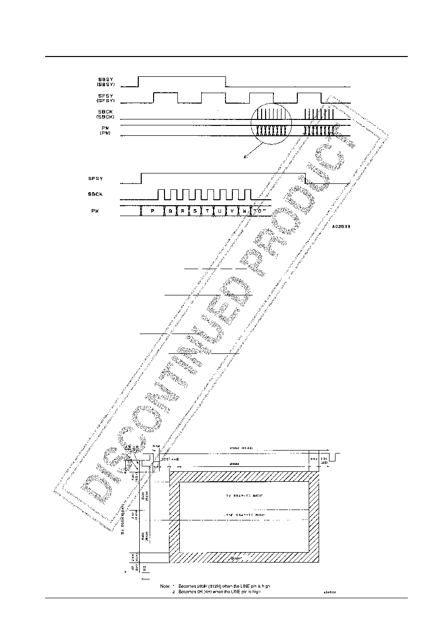
LC7861N/67 interface (Pin names in parentheses are DSP pins.)
LC7868/69/681 interface
Identical to the LC7861N/67 interface except that the SBCK polarity is reversed (the shift occurs on the rising
edge).
3. DRAM Interface; A0 to A7, DB0 to DB3, RAS, CAS, WE, OE
The LC7872E uses an external 64-kword × 4-bit DRAM.
4. Display Format; DEN, N/P1, N/P2, CSYNC, VRESET, HRESET, YS, VIDEO, PALID and TRANS0 to TRANS5
Data to which error detection and correction has been applied is encoded by the RGB encoder and the 8-bit D/A
converter output is output from the VIDEO pin. This circuit handles both NTSC and PAL formats and either mode
can be specified using the N/P pins. See item 1 for details on the pin states for the NTSC and PAL specifications.
The 4FSC2, FSCIN, YS, VRESET, HRESET, PALID and TRANS0 to TRANS5 pins are used in superimposition
mode. The image may be disrupted if the VRESET and HRESET signals are not synchronized with 4FSC2.
The PALID pin is controlled in PAL mode, and is used to match the LC7872E burst signal to the burst component
of the external video signal. When this pin is high, the phase of the burst signal changes every horizontal period,
and when this pin is low, the phase does not change.
The YS pin outputs a control signal used to switch between an external video signal and the LC7872E video signal.
The output conditions for this signal are set by the 2N byte command input registers 0, E, F, and G. The pins
TRANS0 through TRANS5 output signals according to the define transparency instruction.
The DEN pin is a display control pin. The internal font data is output when DEN is low and the color data set up in
the registers is used when DEN is high. The default state is blue.
No. 4868-12/17
LC7872E
相關(guān)PDF資料 |
PDF描述 |
|---|---|
| LC7874E | SPECIALTY CONSUMER CIRCUIT, PQFP64 |
| LC78835K | SPECIALTY CONSUMER CIRCUIT, PDIP24 |
| LC78835KM | SPECIALTY CONSUMER CIRCUIT, PDSO24 |
| LC78845Q | SPECIALTY CONSUMER CIRCUIT, PQFP48 |
| LC80101M | SPECIALTY CONSUMER CIRCUIT, PDSO28 |
相關(guān)代理商/技術(shù)參數(shù) |
參數(shù)描述 |
|---|---|
| LC7874E | 制造商:SANYO 制造商全稱:Sanyo Semicon Device 功能描述:CD Graphics Decorder |
| LC7876E | 制造商:未知廠家 制造商全稱:未知廠家 功能描述: |
| LC7880 | 制造商:SANYO 制造商全稱:Sanyo Semicon Device 功能描述:16 bit D/A CONVERTER |
| LC7880M | 制造商:SANYO 制造商全稱:Sanyo Semicon Device 功能描述:16 bit D/A CONVERTER |
| LC7881 | 制造商:SANYO 制造商全稱:Sanyo Semicon Device 功能描述:CMOS LSI |
發(fā)布緊急采購(gòu),3分鐘左右您將得到回復(fù)。