- 您現(xiàn)在的位置:買賣IC網(wǎng) > PDF目錄377635 > LFECP6E-5F256I (Lattice Semiconductor Corporation) LatticeECP/EC Family Data Sheet PDF資料下載
參數(shù)資料
| 型號(hào): | LFECP6E-5F256I |
| 廠商: | Lattice Semiconductor Corporation |
| 英文描述: | LatticeECP/EC Family Data Sheet |
| 中文描述: | LatticeECP / EC的系列數(shù)據(jù)手冊(cè) |
| 文件頁(yè)數(shù): | 16/117頁(yè) |
| 文件大小: | 557K |
| 代理商: | LFECP6E-5F256I |
第1頁(yè)第2頁(yè)第3頁(yè)第4頁(yè)第5頁(yè)第6頁(yè)第7頁(yè)第8頁(yè)第9頁(yè)第10頁(yè)第11頁(yè)第12頁(yè)第13頁(yè)第14頁(yè)第15頁(yè)當(dāng)前第16頁(yè)第17頁(yè)第18頁(yè)第19頁(yè)第20頁(yè)第21頁(yè)第22頁(yè)第23頁(yè)第24頁(yè)第25頁(yè)第26頁(yè)第27頁(yè)第28頁(yè)第29頁(yè)第30頁(yè)第31頁(yè)第32頁(yè)第33頁(yè)第34頁(yè)第35頁(yè)第36頁(yè)第37頁(yè)第38頁(yè)第39頁(yè)第40頁(yè)第41頁(yè)第42頁(yè)第43頁(yè)第44頁(yè)第45頁(yè)第46頁(yè)第47頁(yè)第48頁(yè)第49頁(yè)第50頁(yè)第51頁(yè)第52頁(yè)第53頁(yè)第54頁(yè)第55頁(yè)第56頁(yè)第57頁(yè)第58頁(yè)第59頁(yè)第60頁(yè)第61頁(yè)第62頁(yè)第63頁(yè)第64頁(yè)第65頁(yè)第66頁(yè)第67頁(yè)第68頁(yè)第69頁(yè)第70頁(yè)第71頁(yè)第72頁(yè)第73頁(yè)第74頁(yè)第75頁(yè)第76頁(yè)第77頁(yè)第78頁(yè)第79頁(yè)第80頁(yè)第81頁(yè)第82頁(yè)第83頁(yè)第84頁(yè)第85頁(yè)第86頁(yè)第87頁(yè)第88頁(yè)第89頁(yè)第90頁(yè)第91頁(yè)第92頁(yè)第93頁(yè)第94頁(yè)第95頁(yè)第96頁(yè)第97頁(yè)第98頁(yè)第99頁(yè)第100頁(yè)第101頁(yè)第102頁(yè)第103頁(yè)第104頁(yè)第105頁(yè)第106頁(yè)第107頁(yè)第108頁(yè)第109頁(yè)第110頁(yè)第111頁(yè)第112頁(yè)第113頁(yè)第114頁(yè)第115頁(yè)第116頁(yè)第117頁(yè)
2-13
Architecture
Lattice Semiconductor
LatticeECP/EC Family Data Sheet
Memory Cascading
Larger and deeper blocks of RAMs can be created using EBR sysMEM Blocks. Typically, the Lattice design tools
cascade memory transparently, based on speci
fi
c design inputs.
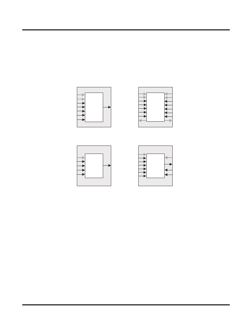
Single, Dual and Pseudo-Dual Port Modes
Figure 2-15 shows the four basic memory con
fi
gurations and their input/output names. In all the sysMEM RAM
modes the input data and address for the ports are registered at the input of the memory array. The output data of
the memory is optionally registered at the output.
Figure 2-15. sysMEM EBR Primitives
The EBR memory supports three forms of write behavior for single port or dual port operation:
1.
Normal
address) does not appear on the output.
– data on the output appears only during read cycle. During a write cycle, the data (at the current
2.
Write Through
– a copy of the input data appears at the output of the same port, during a write cycle.
3.
Read-Before-Write
– when new data is being written, the old content of the address appears at the output.
Memory Core Reset
The memory array in the EBR utilizes latches at the A and B output ports. These latches can be reset asynchro-
nously or synchronously. RSTA and RSTB are local signals, which reset the output latches associated with Port A
and Port B respectively. The Global Reset (GSRN) signal resets both ports. The output data latches and associated
resets for both ports are as shown in Figure 2-16.
EBR
AD[12:0]
DI[35:0]
CLK
CE
RST
WE
CS[2:0]
DO[35:0]
Single Port RAM
EBR
True Dual Port RAM
Pseudo-Dual Port RAM
ROM
AD[12:0]
CLK
CE
RST
DO[35:0]
CS[2:0]
EBR
EBR
ADA[12:0]
DIA[17:0]
CLKA
CEA
RSTA
WEA
CSA[2:0]
DOA[17:0]
ADB[12:0]
DIB[17:0]
CEB
CLKB
RSTB
WEB
CSB[2:0]
DOB[17:0]
ADW[12:0]
DI[35:0]
CLKW
CEW
WE
RST
CS[2:0]
ADR[12:0]
DO[35:0]
CER
CLKR
相關(guān)PDF資料 |
PDF描述 |
|---|---|
| LFECP6E-5F484C | Precision Chopper-Stabilized Operational Amplifier 8-SOIC |
| LFECP6E-5F484I | LatticeECP/EC Family Data Sheet |
| LFECP6E-5F672I | LatticeECP/EC Family Data Sheet |
| LFECP6E-5F900I | LatticeECP/EC Family Data Sheet |
| LFECP6E-5T100C | Precision Chopper-Stabilized Operational Amplifier 14-PDIP |
相關(guān)代理商/技術(shù)參數(shù) |
參數(shù)描述 |
|---|---|
| LFECP6E-5F484C | 功能描述:FPGA - 現(xiàn)場(chǎng)可編程門陣列 6.1 LUT 224 I/O RoHS:否 制造商:Altera Corporation 系列:Cyclone V E 柵極數(shù)量: 邏輯塊數(shù)量:943 內(nèi)嵌式塊RAM - EBR:1956 kbit 輸入/輸出端數(shù)量:128 最大工作頻率:800 MHz 工作電源電壓:1.1 V 最大工作溫度:+ 70 C 安裝風(fēng)格:SMD/SMT 封裝 / 箱體:FBGA-256 |
| LFECP6E-5F484I | 制造商:LATTICE 制造商全稱:Lattice Semiconductor 功能描述:LatticeECP/EC Family Data Sheet |
| LFECP6E-5F672C | 制造商:LATTICE 制造商全稱:Lattice Semiconductor 功能描述:LatticeECP/EC Family Data Sheet |
| LFECP6E-5F672I | 制造商:LATTICE 制造商全稱:Lattice Semiconductor 功能描述:LatticeECP/EC Family Data Sheet |
| LFECP6E-5F900C | 制造商:LATTICE 制造商全稱:Lattice Semiconductor 功能描述:LatticeECP/EC Family Data Sheet |
發(fā)布緊急采購(gòu),3分鐘左右您將得到回復(fù)。