- 您現(xiàn)在的位置:買賣IC網(wǎng) > PDF目錄358821 > LM2576D2T-12 (MOTOROLA INC) EASY SWITCHERE⑩ 3.0 A STEP-DOWN VOLTAGE REGULATOR PDF資料下載
參數(shù)資料
| 型號: | LM2576D2T-12 |
| 廠商: | MOTOROLA INC |
| 元件分類: | 穩(wěn)壓器 |
| 英文描述: | EASY SWITCHERE⑩ 3.0 A STEP-DOWN VOLTAGE REGULATOR |
| 中文描述: | 3 A SWITCHING REGULATOR, 63 kHz SWITCHING FREQ-MAX, PSSO5 |
| 封裝: | PLASTIC, D2PAK-5 |
| 文件頁數(shù): | 18/26頁 |
| 文件大?。?/td> | 278K |
| 代理商: | LM2576D2T-12 |
第1頁第2頁第3頁第4頁第5頁第6頁第7頁第8頁第9頁第10頁第11頁第12頁第13頁第14頁第15頁第16頁第17頁當(dāng)前第18頁第19頁第20頁第21頁第22頁第23頁第24頁第25頁第26頁
LM2576
http://onsemi.com
18
beyond approximately 6.0 in
2
(4000 mm
2
) will not improve
heat
dissipation
significantly.
improvements are needed, double sided or multilayer PC
boards with large copper areas should be considered. In
order to achieve the best thermal performance, it is highly
recommended to use wide copper traces as well as large
areas of copper in the printed circuit board layout. The only
exception to this is the OUTPUT (switch) pin, which should
not have large areas of copper (see page 8 ‘PCB Layout
Guideline’).
If
further
thermal
Thermal Analysis and Design
The following procedure must be performed to determine
whether or not a heatsink will be required. First determine:
1. P
D(max)
maximum regulator power dissipation in the
application.
2. T
A(max
)
maximum ambient temperature in the
application.
3. T
J(max)
maximum allowed junction temperature
(125
°
C for the LM2576). For a conservative
design, the maximum junction temperature
should not exceed 110
°
C to assure safe
operation. For every additional +10
°
C
temperature rise that the junction must
withstand, the estimated operating lifetime
of the component is halved.
4. R
JC
package thermal resistance junctioncase.
5. R
JA
package thermal resistance junctionambient.
(Refer to Maximum Ratings on page 2 of this data sheet or
R
JC
and R
JA
values).
The following formula is to calculate the approximate
total power dissipated by the LM2576:
P
D
= (V
in
x I
Q
) + d x I
Load
x V
sat
where d is the duty cycle and for buck converter
d
ton
T
VO
Vin
,
I
Q
(quiescent current) and V
sat
can be found in the
LM2576 data sheet,
is minimum input voltage applied,
is the regulator output voltage,
I
Load
is the load current.
The dynamic switching losses during turnon and
turnoff can be neglected if proper type catch diode is used.
V
in
V
O
Packages Not on a Heatsink (FreeStanding)
For a freestanding application when no heatsink is used,
the junction temperature can be determined by the following
expression:
T
J
= (R
JA
) (P
D
) + T
A
where (R
JA
)(P
D
) represents the junction temperature rise
caused by the dissipated power and T
A
is the maximum
ambient temperature.
Packages on a Heatsink
If the actual operating junction temperature is greater than
the selected safe operating junction temperature determined
in step 3, than a heatsink is required. The junction
temperature will be calculated as follows:
T
J
= P
D
(R
JA
+ R
CS
+ R
SA
) + T
A
where
R
JC
is the thermal resistance junctioncase,
R
CS
is the thermal resistance caseheatsink,
R
SA
is the thermal resistance heatsinkambient.
If the actual operating temperature is greater than the
selected safe operating junction temperature, then a larger
heatsink is required.
Some Aspects That can Influence Thermal Design
It should be noted that the package thermal resistance and
the junction temperature rise numbers are all approximate,
and there are many factors that will affect these numbers,
such as PC board size, shape, thickness, physical position,
location, board temperature, as well as whether the
surrounding air is moving or still.
Other factors are trace width, total printed circuit copper
area, copper thickness, single or doublesided, multilayer
board, the amount of solder on the board or even color of the
traces.
The size, quantity and spacing of other components on the
board can also influence its effectiveness to dissipate the heat.
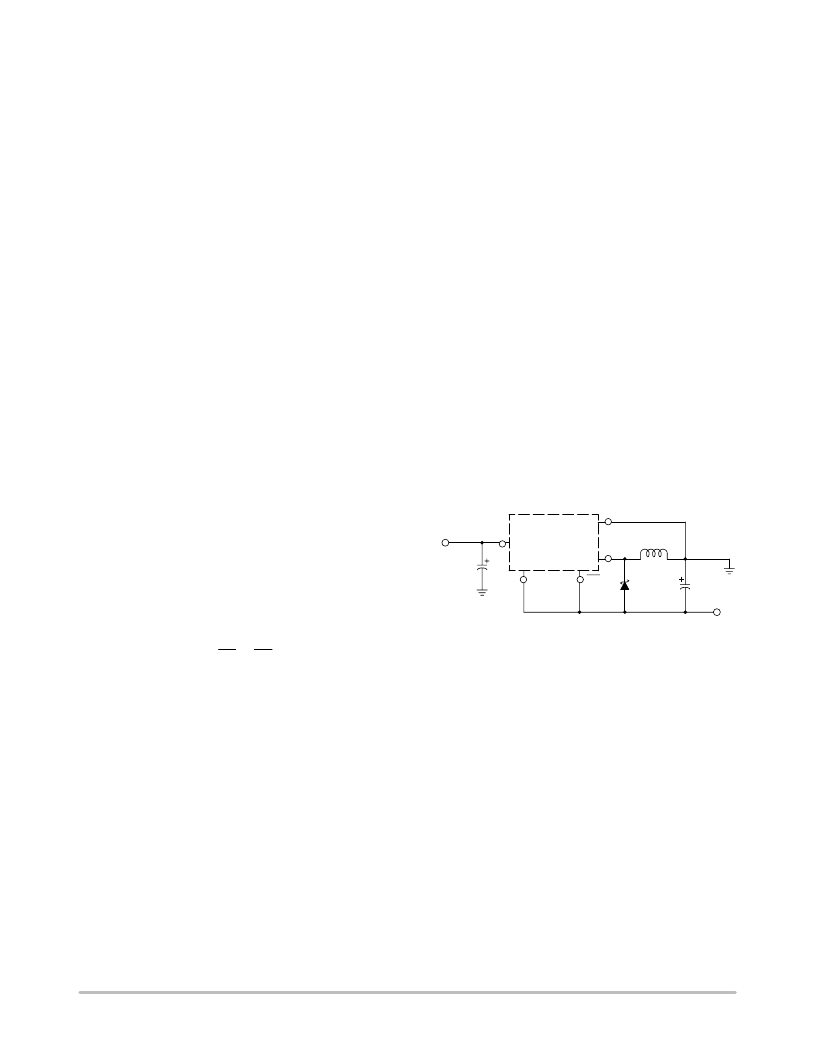
Figure 26. Inverting BuckBoost Develops 12 V
D1
1N5822
L1
68 H
Output
2
4
Feedback
12 to 40 V
Unregulated
DC Input
C
in
100 F
1
5
3
ON/OFF
GN
D
+V
in
12 V @ 0.7 A
Regulated
Output
C
out
2200 F
LM257612
ADDITIONAL APPLICATIONS
Inverting Regulator
An inverting buckboost regulator using the LM257612
is shown in Figure 26. This circuit converts a positive input
voltage to a negative output voltage with a common ground
by bootstrapping the regulators ground to the negative
output voltage. By grounding the feedback pin, the regulator
senses the inverted output voltage and regulates it.
In this example the LM257612 is used to generate a
12 V output. The maximum input voltage in this case
cannot exceed +28 V because the maximum voltage
appearing across the regulator is the absolute sum of the
input and output voltages and this must be limited to a
maximum of 40 V.
相關(guān)PDF資料 |
PDF描述 |
|---|---|
| LM2576R | 3.0A, 15V, Step-Down Switching Regulator |
| LM2577S-12 | Pressure Transducer, Series 19 mm, Uncompensated, Pressure Range: 0 psi to 100 psi, Absolute, flush mount, 10 Vdc excitation |
| LM2577N-ADJ | Pressure Transducer, Series 19 mm, Compensated, Pressure Range: 0 psi to 200 psi, Absolute, flush mount with flange, 10 Vdc excitation |
| LM2577N-15 | Pressure Transducer, Series 19 mm, Compensated, Pressure Range: 0 psi to 200 psi, Absolute, flush mount, 10 Vdc excitation |
| LM2577N-12 | SIMPLE SWITCHER Step-Up Voltage Regulator |
相關(guān)代理商/技術(shù)參數(shù) |
參數(shù)描述 |
|---|---|
| LM2576D2T-15 | 制造商:MOTOROLA 制造商全稱:Motorola, Inc 功能描述:EASY SWITCHERE⑩ 3.0 A STEP-DOWN VOLTAGE REGULATOR |
| LM2576D2T-15G | 功能描述:直流/直流開關(guān)調(diào)節(jié)器 15V 3A Buck PWM RoHS:否 制造商:International Rectifier 最大輸入電壓:21 V 開關(guān)頻率:1.5 MHz 輸出電壓:0.5 V to 0.86 V 輸出電流:4 A 輸出端數(shù)量: 最大工作溫度: 安裝風(fēng)格:SMD/SMT 封裝 / 箱體:PQFN 4 x 5 |
| LM2576D2T-3.3 | 功能描述:直流/直流開關(guān)調(diào)節(jié)器 3.3V 3A Buck PWM RoHS:否 制造商:International Rectifier 最大輸入電壓:21 V 開關(guān)頻率:1.5 MHz 輸出電壓:0.5 V to 0.86 V 輸出電流:4 A 輸出端數(shù)量: 最大工作溫度: 安裝風(fēng)格:SMD/SMT 封裝 / 箱體:PQFN 4 x 5 |
| LM2576D2T-3.3G | 功能描述:直流/直流開關(guān)調(diào)節(jié)器 3.3V 3A Buck PWM RoHS:否 制造商:International Rectifier 最大輸入電壓:21 V 開關(guān)頻率:1.5 MHz 輸出電壓:0.5 V to 0.86 V 輸出電流:4 A 輸出端數(shù)量: 最大工作溫度: 安裝風(fēng)格:SMD/SMT 封裝 / 箱體:PQFN 4 x 5 |
| LM2576D2T-5 | 制造商:MOTOROLA 制造商全稱:Motorola, Inc 功能描述:Easy Switcher 3.0A Step-Down Voltage Regulator |
發(fā)布緊急采購,3分鐘左右您將得到回復(fù)。