- 您現(xiàn)在的位置:買賣IC網(wǎng) > PDF目錄385477 > LM2647MTC (NATIONAL SEMICONDUCTOR CORP) Dual Synchronous Buck Regulator Controller PDF資料下載
參數(shù)資料
| 型號: | LM2647MTC |
| 廠商: | NATIONAL SEMICONDUCTOR CORP |
| 元件分類: | 穩(wěn)壓器 |
| 英文描述: | Dual Synchronous Buck Regulator Controller |
| 中文描述: | DUAL SWITCHING CONTROLLER, 345 kHz SWITCHING FREQ-MAX, PDSO28 |
| 封裝: | TSSOP-28 |
| 文件頁數(shù): | 2/25頁 |
| 文件大小: | 763K |
| 代理商: | LM2647MTC |
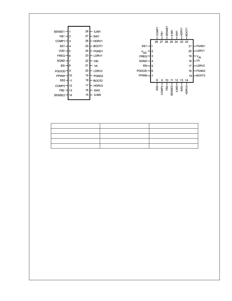
Connection Diagrams
20056302
Top View
28-Lead TSSOP (MTC)
20056303
Top View
28-Lead LLP (LQA)
Ordering Information
Order Number
LM2647MTC
LM2647MTCX
LM2647LQ
LM2647LQX
Package Drawing
MTC28
MTC28
LQA28A
LQA28A
Supplied As
48 Units/Rail
2500 Units/13" Reel
1000 Units/7" Reel
4500 Units/13" Reel
Pin Description
(All pin numbers referred to here correspond to the TSSOP
package)
Pin 1, SENSE1:
Output voltage sense pin for Channel 1. It is
tied directly to the output rail. The SENSE pin voltage is used
together with the VIN voltage (on Pin 22) to (internally)
calculate the CCM (continuous conduction mode) duty cycle.
This calculation is used by the IC to set the minimum duty
cycle in the SKIP mode to 85% of the CCM value. It is also
used to set the adaptive duty cycle clamp (see Pin 3). An
internal 20
resistor from the SENSE pin to ground dis-
charges the output capacitor gently (Soft-shutdown) when-
ever Power Not Good is signaled on Pin 9.
Pin 2, FB1:
Feedback pin for Channel 1. This is the inverting
input of the error amplifier. The voltage on this pin under
regulation is nominally at 0.6V.APower Good window on this
pin determines if the output voltage is within regulation limits
(
±
13%). If the voltage (on either channel) falls outside this
window for more than 7μs, Power Not Good is signaled on
the PGOOD pin (Pin 9). Output over-voltage and under-
voltage conditions are also detected by comparing the volt-
age on the Feedback pin with appropriate internal reference
voltage levels. If the voltage exceeds the safe window
(
±
30%) for longer than 7μs, a fault condition is asserted.
Then both the lower FETs are latched ON and the upper
FETs are latched OFF. When single channel operation is
desired, the Feedback pins of both channels should be
connected together, near the IC. All other pins specific to the
unused channel should be left floating (not connected to
each other either).
Pin 3, COMP1:
Compensation pin for Channel 1. This is also
the output of the error amplifier of this channel. The voltage
level on this pin is compared with an internally generated
ramp signal to set the duty cycle for normal regulation. Since
the Feedback pin is the inverting input of the same error
amplifier, appropriate control loop compensation compo-
nents are placed between this pin and the Feedback pin.
The COMP pin is internally pulled low during Soft-start so as
to limit the duty cycle. Once Soft-start is completed, the
voltage on this pin can take up the value required to maintain
output regulation. But an internal voltage clamp does not
allow the pin to go much higher than the steady-state re-
quirement. This forms the adaptive duty cycle clamp feature
which serves to limit the maximum allowable duty cycle and
peak currents under sudden overloads. But at the same time
it has enough headroom to permit an adequate response to
step loads within the normal operating range.
Pin 4, SS1:
Channel 1 Soft-start pin. A Soft-start capacitor is
placed between this pin and ground. A typical capacitance of
0.1μF is always recommended between this pin and ground.
The IC connects an internal 1.8 k
resistor (R
SS_DCHG
, see
Electrical Characteristics table) between this pin and ground
to discharge any remaining charge on the Soft-start capaci-
tor under several conditions. These conditions include the
initial power-up sequence, start-up by toggling the EN pin,
and also recovery from a fault condition. The purpose is to
bring down the voltage on both the Soft-start pins to below
100mV for obtaining reset. Reset having thus been obtained,
an 11μA current source at this pin charges up the Soft-start
capacitor. The voltage on this pin controls the maximum duty
cycle, and this produces a gradual ramp-up of the output
voltage, thereby preventing large inrush currents into the
L
www.national.com
2
相關(guān)PDF資料 |
PDF描述 |
|---|---|
| LM2665M6 | Switched Capacitor Voltage Converter |
| LM2665M6X | Switched Capacitor Voltage Converter |
| LM2707 | Inductive-Boost Series LED Driver with Programmable Oscillator Frequency |
| LM2707MF | Inductive-Boost Series LED Driver with Programmable Oscillator Frequency |
| LM2707MFX | Inductive-Boost Series LED Driver with Programmable Oscillator Frequency |
相關(guān)代理商/技術(shù)參數(shù) |
參數(shù)描述 |
|---|---|
| LM2647MTC/NOPB | 功能描述:DC/DC 開關(guān)控制器 RoHS:否 制造商:Texas Instruments 輸入電壓:6 V to 100 V 開關(guān)頻率: 輸出電壓:1.215 V to 80 V 輸出電流:3.5 A 輸出端數(shù)量:1 最大工作溫度:+ 125 C 安裝風(fēng)格: 封裝 / 箱體:CPAK |
| LM2647MTCX | 功能描述:DC/DC 開關(guān)控制器 RoHS:否 制造商:Texas Instruments 輸入電壓:6 V to 100 V 開關(guān)頻率: 輸出電壓:1.215 V to 80 V 輸出電流:3.5 A 輸出端數(shù)量:1 最大工作溫度:+ 125 C 安裝風(fēng)格: 封裝 / 箱體:CPAK |
| LM2647MTCX/NOPB | 功能描述:DC/DC 開關(guān)控制器 RoHS:否 制造商:Texas Instruments 輸入電壓:6 V to 100 V 開關(guān)頻率: 輸出電壓:1.215 V to 80 V 輸出電流:3.5 A 輸出端數(shù)量:1 最大工作溫度:+ 125 C 安裝風(fēng)格: 封裝 / 箱體:CPAK |
| LM2648 | 制造商:NSC 制造商全稱:National Semiconductor 功能描述:Two-Phase, Synchronous Step-Down 3-Channel Switching Regulator Controller |
| LM26480 | 制造商:NSC 制造商全稱:National Semiconductor 功能描述:Externally Programmable Dual High-Current Step-Down DC/DC and Dual Linear Regulators |
發(fā)布緊急采購,3分鐘左右您將得到回復(fù)。