- 您現(xiàn)在的位置:買賣IC網(wǎng) > PDF目錄361035 > LM9811CCV (NATIONAL SEMICONDUCTOR CORP) 10-Bit Greyscale/30-Bit Color Linear CCD Sensor Processor PDF資料下載
參數(shù)資料
| 型號(hào): | LM9811CCV |
| 廠商: | NATIONAL SEMICONDUCTOR CORP |
| 元件分類: | 模擬信號(hào)調(diào)理 |
| 英文描述: | 10-Bit Greyscale/30-Bit Color Linear CCD Sensor Processor |
| 中文描述: | SPECIALTY ANALOG CIRCUIT, PQCC52 |
| 封裝: | PLASTIC, LCC-52 |
| 文件頁數(shù): | 28/36頁 |
| 文件大?。?/td> | 605K |
| 代理商: | LM9811CCV |
第1頁第2頁第3頁第4頁第5頁第6頁第7頁第8頁第9頁第10頁第11頁第12頁第13頁第14頁第15頁第16頁第17頁第18頁第19頁第20頁第21頁第22頁第23頁第24頁第25頁第26頁第27頁當(dāng)前第28頁第29頁第30頁第31頁第32頁第33頁第34頁第35頁第36頁
Applications Information
(Continued)
even with the VGA gain set to a maximum of 2.8, the ampli-
tude of one or more pixels is less than the minimum required
for shading correction. The solution is to increase the inten-
sity of the light source or lengthen the integration time of the
CCD to increase the CCD’s output amplitude.
To ensure that a scanner system is manufacturable, the re-
sult of the VGA calibration must always be State 1. States 2,
3, and 4 must be eliminated either by ensuring that the total
variation in light intensity (from all sources) from system to
system to a maximum of 9 dB, or by being able to adjust the
light source’s intensity and/or the CCD’s light integration
time.
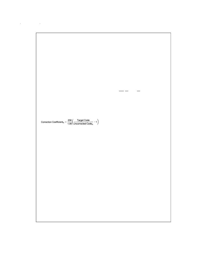
5.3 PGA Correction Coefficients (Shading Calibration)
Once the input signal has been centered inside the range the
LM9811 can correct for, correction coefficients must be gen-
erated for each pixel to compensate for the gain error of that
pixel.
1.
Set Offset DAC and Add Bit as determined in Section
5.1.
2.
Set the VGAgain to the value determined in Section 5.2.
3.
Set the PGA gain to 0 dB.
4.
Scan a reference line corresponding to all white or light
grey and store it in memory.
5.
Calculate the required gain correction coefficients for
each pixel using the formula:
Where
Uncorrected Code
n
is the ADC output code for pixel
n with the PGA gain = 0 dB,
Target Code
is the number that
corresponds to the desired output from the ADC with the
given reference line input, and
Correction Coefficient
is
the gain correction number that is sent to the CD0–CD7 cor-
rection databus to provide gain correction for pixel n when
digitizing a line with the LM9811’s PGA gain correction oper-
ating.
If it is difficult or undesirable to do the division, subtraction,
and multiplication operations shown above for every pixel,
then a lookup table can be generated in advance that will re-
turn the Correction Coefficient for any Uncorrected Code.
This table can be stored in ROM or RAM and can speed up
the calibration process. The disadvantage of this technique
is that the Target Code must be fixed when the table is gen-
erated, so only one Target Code can be used (unless mul-
tiple tables are generated).
All the Correction Coefficients must be stored and sent to the
LM9811 through the CD0–CD7 databus for every line
scanned.
6.0 POWER SUPPLY CONSIDERATIONS
6.1 General
The LM9811 should be powered by a single +5V source (un-
less 3V-compatible digital I/O is required— see Section 6.2).
The analog supplies (V
) and the digital supplies (V
and
V
) are brought out individually to allow separate by-
passing for each supply input. They should not be powered
by two or more different supplies.
In systems with separate analog and digital +5V supplies, all
the supply pins of the LM9811 should be powered by the
analog +5V supply. Each supply input should be bypassed to
its respective ground with a 0.1 μF capacitor located as close
as possible to the supply input pin. A single 10 μF tantalum
should be placed near the V
A
supply pin to provide low fre-
quency bypassing.
To minimize noise, keep the LM9811 and all analog compo-
nents as far as possible from noise generators, such as
switching power supplies and high frequency digital busses.
If possible, isolate all the analog components and signals
(OS, reference inputs and outputs, V
, AGND) on an analog
ground plane, separate from the digital ground plane. The
two ground planes should be tied together at a single point,
preferably the point where the power supply enters the PCB.
6.2 3V Compatible Digital I/O
If 3V digital I/O operation is desired, the V
D(I/O)
pin may be
powered by a separate 3V
±
10% or 3.3V
±
this case, all the digital I/O pins (CD0–CD7, CCLK, MCLK,
DD0–DD9, EOC, RD, SYNC, CS, SCLK, SDO, and SDI) will
be 3V compatible. The CCD clock signals (
φ
1,
φ
2, RS, and
TR) remain 5V outputs, powered by V
D
. In this case the
V
input should be bypassed to DGND
with a parallel
combination of a 0.1 μF capacitor and a 10 μF tantalum ca-
pacitor.
6.3 Power Down Mode
Setting the Power Down bit to a “1” puts the device in a low
power standby mode. The CCD outputs (
φ
1,
φ
2, RS, and TR)
are pulled low and the analog sections are turned off to con-
serve power. The digital logic will continue to operate if
MCLK continues and SYNC is held high, so for minimum
power dissipation MCLK should be stopped when the
LM9811 enters the Power Down mode. Recovery from
Power Down typically takes 50 μs (the time required for the
reference voltages to settle to 0.5 LSB accuracy).
7.0 COLOR
There are two primary ways to use the LM9811 in a color
system with a triple output (RGB) CCD. The first is to use
one LM9801 with an external multiplexer. This is the simplest
solution. The second technique is to use one LM9811 per
RGB color.
7.1 Parallel Output CCD, One LM9811
Figure 31 is an example of how to use a single LM9811 with
a triple-output RGB CCD. In this case an entire line of red is
digitized, followed by an entire line of green, then blue. This
solution provides a 1.5 Mpixels/sec (for an effective 500k
RGB pixels/sec after de-interleaving) pixel rate using a high
performance triple output color CCD.
The Mux 1 multiplexer, located between the CCD’s OS out-
puts and the LM9811’s OS input, selects the color to be digi-
tized according to the states of theAand B inputs (described
below). The multiplexer’s speed requirements are minimal
because the mux switches at the line rate, not the pixel rate.
Also, since the output of the mux goes into a high imped-
ance, low-capacitance input, the ON resistance of the mux is
not critical. The 74HC4052 is a good choice for this
application.
www.national.com
28
相關(guān)PDF資料 |
PDF描述 |
|---|---|
| LM9831CCVJD | LM9831 42-Bit Color, 1200dpi USB Image Scanner |
| LM9831 | LM9831 42-Bit Color, 1200dpi USB Image Scanner |
| LM9831CCVJDX | LM9831 42-Bit Color, 1200dpi USB Image Scanner |
| LM9832CCVJD | LM9832 42-Bit Color, 1200dpi USB Image Scanner |
| LM9832 | LM9832 42-Bit Color, 1200dpi USB Image Scanner |
相關(guān)代理商/技術(shù)參數(shù) |
參數(shù)描述 |
|---|---|
| LM9811CCVF | 制造商:NSC 制造商全稱:National Semiconductor 功能描述:10-Bit Greyscale/30-Bit Color Linear CCD Sensor Processor |
| LM9812 | 制造商:NSC 制造商全稱:National Semiconductor 功能描述:LM9812 30-Bit Color Linear CCD Sensor Processor |
| LM9812CCV | 制造商:NSC 制造商全稱:National Semiconductor 功能描述:LM9812 30-Bit Color Linear CCD Sensor Processor |
| LM981-SC36 | 功能描述:基本/快動(dòng)開關(guān) Foot Switch RoHS:否 制造商:Omron Electronics 觸點(diǎn)形式:SPDT 執(zhí)行器:Lever 電流額定值:5 A 電壓額定值 AC:250 V 電壓額定值 DC:30 V 功率額定值: 工作力:120 g IP 等級(jí):IP 67 NEMA 額定值: 端接類型:Wire 安裝:Panel |
| LM981-ZZ | 功能描述:基本/快動(dòng)開關(guān) Foot Switch RoHS:否 制造商:Omron Electronics 觸點(diǎn)形式:SPDT 執(zhí)行器:Lever 電流額定值:5 A 電壓額定值 AC:250 V 電壓額定值 DC:30 V 功率額定值: 工作力:120 g IP 等級(jí):IP 67 NEMA 額定值: 端接類型:Wire 安裝:Panel |
發(fā)布緊急采購(gòu),3分鐘左右您將得到回復(fù)。