- 您現(xiàn)在的位置:買賣IC網(wǎng) > PDF目錄358885 > LMV721M5X (NATIONAL SEMICONDUCTOR CORP) 10MHz, Low Noise, Low Voltage, and Low Power Operational Amplifier PDF資料下載
參數(shù)資料
| 型號: | LMV721M5X |
| 廠商: | NATIONAL SEMICONDUCTOR CORP |
| 元件分類: | 運(yùn)動控制電子 |
| 英文描述: | 10MHz, Low Noise, Low Voltage, and Low Power Operational Amplifier |
| 中文描述: | OP-AMP, 3000 uV OFFSET-MAX, 10 MHz BAND WIDTH, PDSO5 |
| 封裝: | SOT-23, 5 PIN |
| 文件頁數(shù): | 8/15頁 |
| 文件大小: | 459K |
| 代理商: | LMV721M5X |
Typical Performance characteristics
(Continued)
Application Notes
1.0 Benefits of the LMV721/722 Size.
The small footprints of the LMV721/722 packages save
space on printed circuit boards, and enable the design of
smaller electronic products, such as cellular phones, pagers,
or
other
portable
systems.
LMV721/722 make them possible to use in PCMCIA type III
cards.
Signal Integrity.
Signals can pick up noise between the sig-
nal source and the amplifier. By using a physically smaller
amplifier package, the LMV721/722 can be placed closer to
the signal source, reducing noise pickup and increasing sig-
nal integrity.
Simplified Board Layout.
These products help you to avoid
using long pc traces in your pc board layout. This means that
no additional components, such as capacitors and resistors,
are needed to filter out the unwanted signals due to the inter-
ference between the long pc traces.
Low Supply Current.
These devices will help you to maxi-
mize battery life. They are ideal for battery powered sys-
tems.
Low Supply Voltage.
National provides guaranteed perfor-
mance at 2.2V and 5V. These guarantees ensure operation
throughout the battery lifetime.
Rail-to-Rail Output.
Rail-to-rail output swing provides maxi-
mum possible dynamic range at the output. This is particu-
larly important when operating on low supply voltages.
Input Includes Ground.
Allows direct sensing near GND in
single supply operation.
Protection should be provided to prevent the input voltages
from going negative more than 0.3V (at 25C). An input
clamp diode with a resistor to the IC input terminal can be
used.
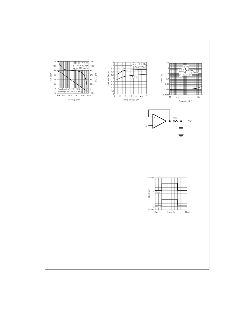
2.0 Capacitive Load Tolerance
The LMV721/722 can directly drive 4700pF in unity-gain
without oscillation. The unity-gain follower is the most sensi-
tive configuration to capacitive loading. Direct capacitive
loading reduces the phase margin of amplifiers. The combi-
nation of the amplifier’s output impedance and the capacitive
load induces phase lag. This results in either an under-
damped pulse response or oscillation. To drive a heavier ca-
pacitive load, circuit in Figure 1 can be used.
The
low
profile
of
the
In Figure 1 the isolation resistor R
and the load capacitor
C
form a pole to increase stability by adding more phase
margin to the overall system. the desired performance de-
pends on the value of R
ISO
. The bigger the R
resistor
value, the more stable V
will be. Figure 2 is an output
waveform of Figure 1 using 100k
for R
ISO
and 2000μF for
C
L
.
The circuit in Figure 3is an improvement to the one in Figure
1 because it provides DC accuracy as well as AC stability. If
there were a load resistor in Figure 1 the output would be
voltage divided by R
and the load resistor. Instead, in Fig-
ure 3 R
provides the DC accuracy by using feed-forward
techniques to connect V
to R
. Caution is needed in choos-
ing the value of R
due to the input bias current of the
LMV721/722. C
and R
serve to counteract the loss of
phase margin by feeding the high frequency component of
the output signal back to the amplifier’s inverting input,
thereby preserving phase margin in the overall feedback
Gain and Phase Margin vs.
Frequency (V
S
= 5V, R
L
600
)
DS100922-16
Slew Rate vs.
Supply Voltage
DS100922-17
THD vs.
Frequency
DS100922-42
DS100922-18
FIGURE 1. Indirectly Driving A capacitive Load Using
Resistive Isolation
DS100922-31
FIGURE 2. Pulse Response of the LMV721 Circuit in
Figure 1
www.national.com
8
相關(guān)PDF資料 |
PDF描述 |
|---|---|
| LMV721M5 | 10MHz, Low Noise, Low Voltage, and Low Power Operational Amplifier |
| LMV7239 | 45ns, Ultra Low Power, Low Voltage, Rail-to-Rail Input Comparator with Open-Drain/Push-Pull Output |
| LMV7239M5 | DIODE ZENER SINGLE 200mW 11Vz 20mA-Izt 0.05 2uA-Ir 8.4 SOT-323 3K/REEL |
| LMV7239M5X | 45ns, Ultra Low Power, Low Voltage, Rail-to-Rail Input Comparator with Open-Drain/Push-Pull Output |
| LMV7239M7 | DIODE ZENER SINGLE 350mW 12Vz 20mA-Izt 0.05 1uA-Ir 9.1 SOT-23 3K/REEL |
相關(guān)代理商/技術(shù)參數(shù) |
參數(shù)描述 |
|---|---|
| LMV721M5X/NOPB | 功能描述:運(yùn)算放大器 - 運(yùn)放 RoHS:否 制造商:STMicroelectronics 通道數(shù)量:4 共模抑制比(最小值):63 dB 輸入補(bǔ)償電壓:1 mV 輸入偏流(最大值):10 pA 工作電源電壓:2.7 V to 5.5 V 安裝風(fēng)格:SMD/SMT 封裝 / 箱體:QFN-16 轉(zhuǎn)換速度:0.89 V/us 關(guān)閉:No 輸出電流:55 mA 最大工作溫度:+ 125 C 封裝:Reel |
| LMV721M7 | 功能描述:運(yùn)算放大器 - 運(yùn)放 RoHS:否 制造商:STMicroelectronics 通道數(shù)量:4 共模抑制比(最小值):63 dB 輸入補(bǔ)償電壓:1 mV 輸入偏流(最大值):10 pA 工作電源電壓:2.7 V to 5.5 V 安裝風(fēng)格:SMD/SMT 封裝 / 箱體:QFN-16 轉(zhuǎn)換速度:0.89 V/us 關(guān)閉:No 輸出電流:55 mA 最大工作溫度:+ 125 C 封裝:Reel |
| LMV721M7 | 制造商:Texas Instruments 功能描述:OP AMP ULTRA LOW NOISE POWERWISE |
| LMV721M7/NOPB | 功能描述:運(yùn)算放大器 - 運(yùn)放 Ultra Low Noise Sgl Op Amp RoHS:否 制造商:STMicroelectronics 通道數(shù)量:4 共模抑制比(最小值):63 dB 輸入補(bǔ)償電壓:1 mV 輸入偏流(最大值):10 pA 工作電源電壓:2.7 V to 5.5 V 安裝風(fēng)格:SMD/SMT 封裝 / 箱體:QFN-16 轉(zhuǎn)換速度:0.89 V/us 關(guān)閉:No 輸出電流:55 mA 最大工作溫度:+ 125 C 封裝:Reel |
| LMV721M7X | 功能描述:運(yùn)算放大器 - 運(yùn)放 RoHS:否 制造商:STMicroelectronics 通道數(shù)量:4 共模抑制比(最小值):63 dB 輸入補(bǔ)償電壓:1 mV 輸入偏流(最大值):10 pA 工作電源電壓:2.7 V to 5.5 V 安裝風(fēng)格:SMD/SMT 封裝 / 箱體:QFN-16 轉(zhuǎn)換速度:0.89 V/us 關(guān)閉:No 輸出電流:55 mA 最大工作溫度:+ 125 C 封裝:Reel |
發(fā)布緊急采購,3分鐘左右您將得到回復(fù)。