- 您現(xiàn)在的位置:買賣IC網(wǎng) > PDF目錄367589 > LS5540-7R 100 Watt AC-DC Converters with PFC PDF資料下載
參數(shù)資料
| 型號: | LS5540-7R |
| 英文描述: | 100 Watt AC-DC Converters with PFC |
| 中文描述: | 100瓦交直流轉(zhuǎn)換器的功率因數(shù)校正 |
| 文件頁數(shù): | 23/27頁 |
| 文件大小: | 599K |
| 代理商: | LS5540-7R |
第1頁第2頁第3頁第4頁第5頁第6頁第7頁第8頁第9頁第10頁第11頁第12頁第13頁第14頁第15頁第16頁第17頁第18頁第19頁第20頁第21頁第22頁當(dāng)前第23頁第24頁第25頁第26頁第27頁

Cassette Style
100 Watt AC-DC Converters
S Series PFC
Edition 01/01.2001
23/27
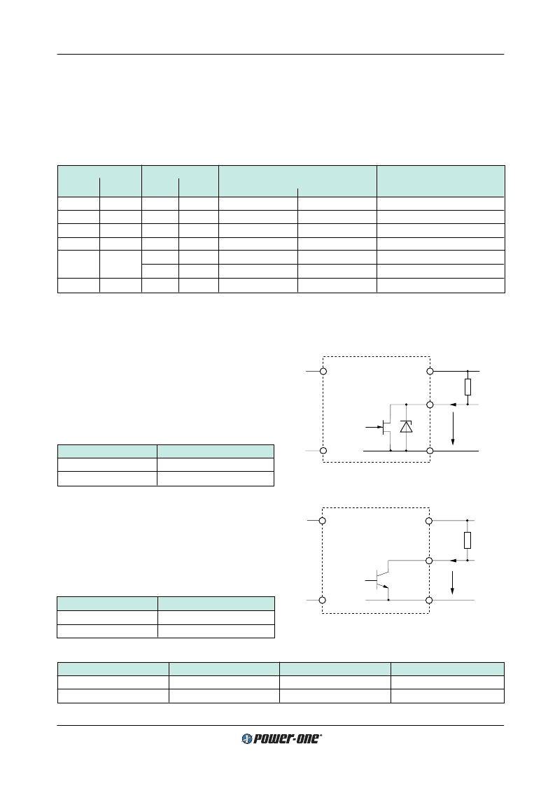
Table 19: D-output logic signals
Version of D
U
i
<
U
t
resp. U
o
<
U
t
U
i
>
U
t
+ U
h
resp. U
o
>
U
t
Con
fi
guration
D1, D2, D3, D4, D0
low
high
JFET
D5, D6, D7, D8, D9, DD
high
low
NPN
D Undervoltage Monitor
The input and/or output undervoltage monitoring circuit op-
erates independently of the built-in input undervoltage lock-
out circuit. A logic "low" (JFET output) or "high" signal (NPN
output) s generated at pin 20 as soon as one of the moni-
tored voltages drops below the preselected threshold level
U
t
. The return for this signal is Vo1
–
. The D output recovers
when the monitored voltage(s) exceed(s) U
t
+ U
h
. The
Table 18: Undervoltage monitoring functions
Output type
JFET
Monitoring
U
i
Minimum adjustment range
of threshold level U
t
U
ti
Typical hysteresis U
ho
[% of U
t
]
for U
t min
...U
t max
U
ho
NPN
U
o1
U
to
D1
D5
no
yes
-
3.5...40 V
1
2.5...0.6
D2
D6
yes
no
355V DC
4
-
-
D3
D7
yes
yes
355V DC
4
(0.95...0.985 U
o1
)
2
"0"
D4
D8
no
yes
-
(0.95...0.985 U
o1
)
2
"0"
D0
D9
no
yes
-
3.5...40 V
3
2.5...0.6
yes
yes
355V DC
4
3.5...40 V
3
2.5...0.6
DD
yes
yes
355V DC
4
3.5...40 V
1
2.5...0.6
1
Threshold level adjustable by potentiometer
2
Fixed value. Tracking if U
o1
adjusted via R-input, option P or sense lines.
3
The threshold level permanently adjusted according to customer speci
fi
cation
±
2% at 25
°
C. Any value within the speci
fi
ed range is
basically possible but causes a special type designation in addition to the standard option designations (D0/D9)!
4
Option D monitors the boost regulator output voltage. The trigger level is adjusted in the factory to 355 V DC.
threshold level U
ti
is adjusted in the factory. The threshold
level U
to
is either adjusted by a potentiometer, accessible
through a hole in the front cover, or factory adjusted to a
fi
xed value speci
fi
ed by the customer.
Option D exists in various versions D0...DD as shown in the
following table.
Vo1+
Vo1
–
D
U
D
I
D
R
p
I
11007
Vo1+
Vo1
–
D
U
D
I
D
R
p
I
11006
Fig. 36
Option D0...D4: JFET output, I
D
≤
2.5 mA
NPN output (D5...DD):
Connector pin D is internally connected via the collector-
emitter path of a NPN transistor to the negative potential of
output 1. U
D
<
0.4 V (logic low) corresponds to a monitored
voltage level (U
i
and/or U
o1
)
>
U
t
+ U
h
. The current I
D
through the open collector should not exceed 20 mA. The
NPN output is not protected against external overvoltages.
U
D
should not exceed 40 V.
U
i
, U
o1
status
U
i
or U
o1
<
U
t
U
i
and U
o1
>
U
t
+ U
h
D output, U
D
high, H, I
D
≤
25
μ
A at U
D
= 40 V
low, L, U
D
≤
0.4 V at I
D
= 20 mA
JFET output (D0
…
D4):
Connector pin D is internally connected via the drain-
source path of a JFET (self-conducting type) to the nega-
tive potential of output 1. U
D
≤
0.4 V (logic low) corresponds
to a monitored voltage level (U
i
and/or U
o1
)
<
U
t
. The cur-
rent I
D
through the JFET should not exceed 2.5 mA. The
JFET is protected by a 0.5 W Zener diode of 8.2 V against
external overvoltages.
U
i
, U
o1
status
U
i
or U
o1
<
U
t
U
i
and U
o1
>
U
t
+ U
h
D output, U
D
low, L, U
D
≤
0.4 V at I
D
= 2.5 mA
high, H, I
D
≤
25
μ
A at U
D
= 5.25 V
Fig. 37
Option D5...DD: NPN output, U
o1
≤
40 V, I
D
≤
20 mA
相關(guān)PDF資料 |
PDF描述 |
|---|---|
| LS5660-7R | 100 Watt AC-DC Converters with PFC |
| LS4501-7R | 100 Watt AC-DC Converters with PFC |
| LS4601-7R | 100 Watt AC-DC Converters with PFC |
| LS505 | LS505 - Symmetrical peak clipping in a feedback configuration |
| LS505MCRO | Analog IC |
相關(guān)代理商/技術(shù)參數(shù) |
參數(shù)描述 |
|---|---|
| LS5540-9ER | 制造商:Power-One 功能描述:ACDC - Bulk |
| LS5-544 | 功能描述:打印機(jī) LS5, Laminated Continuous Tape, Polyeste RoHS:否 制造商:Seiko Instruments 產(chǎn)品:Printer 電源電壓: 每行點(diǎn)數(shù):9 x 320 打印速度:52.5 cps, 80 cps 紙張寬度:112 mm |
| LS5-547 | 制造商:Panduit Corp 功能描述: |
| LS5-60 | 制造商:Panduit Corp 功能描述: |
| LS-560M2H---2225S | 制造商:Surge Components Inc 功能描述:CAP ALUM 56UF 500V ?20% 2000LHRS 22 X 25 - Bulk |
發(fā)布緊急采購,3分鐘左右您將得到回復(fù)。