- 您現(xiàn)在的位置:買賣IC網(wǎng) > PDF目錄377664 > LS7366R (LSI Corporation) 32-BIT QUADRATURE COUNTER WITH SERIAL INTERFACE PDF資料下載
參數(shù)資料
| 型號(hào): | LS7366R |
| 廠商: | LSI Corporation |
| 元件分類: | 通用總線功能 |
| 英文描述: | 32-BIT QUADRATURE COUNTER WITH SERIAL INTERFACE |
| 中文描述: | 32位正交計(jì)數(shù)器串行接口 |
| 文件頁(yè)數(shù): | 1/13頁(yè) |
| 文件大?。?/td> | 101K |
| 代理商: | LS7366R |
當(dāng)前第1頁(yè)第2頁(yè)第3頁(yè)第4頁(yè)第5頁(yè)第6頁(yè)第7頁(yè)第8頁(yè)第9頁(yè)第10頁(yè)第11頁(yè)第12頁(yè)第13頁(yè)
GENERAL FEATURES:
Operating voltage: 3V to 5.5V (V
DD
- V
SS
)
5V count frequency: 40MHz
3V count frequency: 20MHz
32-bit counter (CNTR).
32-bit data register (DTR) and comparator.
32-bit output register (OTR).
Two 8-bit mode registers (MDR0, MDR1)
for programmable functional modes.
8-bit instruction register (IR).
8-bit status register (STR).
Latched Interrupt output on Carry or Borrow or Compare or Index.
Index driven counter load, output register load or counter reset.
Internal quadrature clock decoder and filter.
x1, x2 or x4 mode of quadrature counting.
Non-quadrature up/down counting.
Modulo-N, Non-recycle, Range-limit or
Free-running modes of counting
8-bit, 16-bit, 24-bit and 32-bit programmable configuration
synchronous (SPI) serial interface
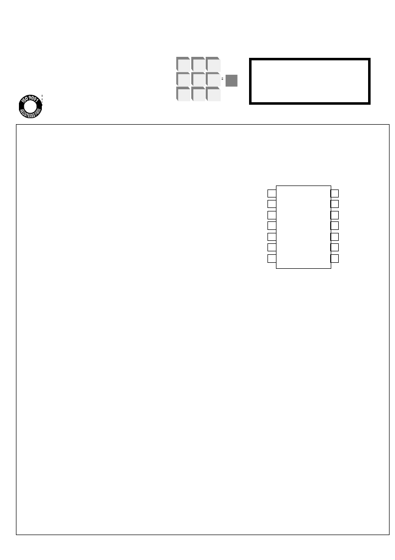
LS7366R (DIP), LS7366R-S (SOIC), LS7366R-TS (TSSOP)
- See Figure 1 -
SPI/MICROWIRE
(Serial Peripheral Interface):
Standard 4-wire connection: MOSI, MISO, SS/ and SCK.
Slave mode only.
GENERAL DESCRIPTION:
LS7366R is a 32-bit CMOS counter, with direct interface for quadra-
ture clocks from incremental encoders. It also interfaces with the
index signals from incremental encoders to perform variety of
marker functions.
For communications with microprocessors or microcontrollers, it
provides a 4-wire SPI/MICROWIRE bus.The four standard bus I/Os
are SS/, SCK, MISO and MOSI. The data transfer between a micro-
controller and a slave LS7366R is synchronous. The synchroniza-
tion is done by the SCK clocks supplied by the microcontroller. Each
transmission is organized in blocks of 1 to 5 bytes of data. A trans-
mission cycle is intitiated by a high to low transition of the SS/ input.
The first byte received in a transmission cycle is always an instruc-
tion byte, whereas the second through the fifth bytes are always
interpreted as data bytes. A transmission cycle is terminated with
the low to high transition of the SS/ input. Received bytes are shifted
in at the MOSI input, MSB first, with the leading edges (high transi-
tion) of the SCK clocks. Output data are shifted out on the MISO
output, MSB first, with the trailing edges (low transition) of the SCK
clocks.
32-BIT QUADRATURE COUNTER WITH SERIAL INTERFACE
LSI/CSI
LSI Computer Systems, Inc. 1235 Walt Whitman Road, Melville, NY 11747 (631) 271-0400 FAX (631) 271-0405
LS7366R
UL
A3800
May 2006
7366R-050106-1
Read and write commands cannot be combined.
For example, when the device is shifting out read
data on MISO output, it ignores the MOSI input,
even though the SS/ input is active. SS/ must be
terminated and reasserted before the device will
accept a new command.
The counter can be configured to operate as 1, 2, 3
or 4-byte counter. When configured as an n-byte
counter, the CNTR, DTR and OTR are all config-
ured as n-byte registers, where n = 1, 2, 3 or 4.
The content of the instruction/data identity is
automatically adjusted to match the n-byte configu-
ration. For example, if the counter is configured as a
2-byte counter, the instruction “write to DTR”
expects 2 data bytes following the instruction byte.
If the counter is configured as a 3-byte counter, the
same instruction will expect 3 bytes of data follow-
ing the instruction byte.
Following the transfer of the appropriate number of
bytes any further attempt of data transfer is ignored
until a new instruction cycle is started by switching
the SS/ input to high and then low.
The counter can be programmed to operate in a
number of different modes, with the operating
characteristics being written into the two mode
registers MDR0 and MDR1. Hardware I/Os are
provided for event driven operations, such as
processor interrupt and index related functions.
1
2
3
4
5
6
7
8
9
10
11
12
13
14
Vss
V
DD
B
A
INDEX/
LFLAG/
SS/
SCK
L
MISO
MOSI
f
CKi
f
CKO
CNT_EN
DFLAG/
FIGURE 1
L
PIN A S S IGNMENT
T OP V IEW
相關(guān)PDF資料 |
PDF描述 |
|---|---|
| LS7534 | DIMMER LIGHT SWITCH WITH UP AND DOWN CONTROLS |
| LS7535 | DIMMER LIGHT SWITCH WITH UP AND DOWN CONTROLS |
| LS7538 | TOUCH CONTROL STEP DIMMER LIGHT SWITCH WITH AUTOMATIC GAIN CONTROL (AGC) |
| LS7539 | TOUCH CONTROL STEP DIMMER LIGHT SWITCH WITH AUTOMATIC GAIN CONTROL (AGC) |
| LS7540 | TOUCH CONTROL CONTINUOUS DIMMER with AUTOMATIC GAIN CONTROL (AGC) |
相關(guān)代理商/技術(shù)參數(shù) |
參數(shù)描述 |
|---|---|
| LS73-680-RM | 制造商:ICE 制造商全稱:ice Components, Ins. 功能描述:Surface Mount Power Inductors |
| LS73-681-RM | 制造商:ICE 制造商全稱:ice Components, Ins. 功能描述:Surface Mount Power Inductors |
| LS7-38-1 | 功能描述:電線鑒定 BLACK/WHITE 3/8" LAMINATED ADH. RoHS:否 制造商:TE Connectivity / Q-Cees 產(chǎn)品:Labels and Signs 類型: 材料:Vinyl 顏色:Blue 寬度:0.625 in 長(zhǎng)度:1 in |
| LS7-38-2 | 功能描述:電線鑒定 BLACK/CLEAR 3/8" LAMINATED ADH. RoHS:否 制造商:TE Connectivity / Q-Cees 產(chǎn)品:Labels and Signs 類型: 材料:Vinyl 顏色:Blue 寬度:0.625 in 長(zhǎng)度:1 in |
| LS73-820-RM | 制造商:ICE 制造商全稱:ice Components, Ins. 功能描述:Surface Mount Power Inductors |
發(fā)布緊急采購(gòu),3分鐘左右您將得到回復(fù)。