- 您現(xiàn)在的位置:買賣IC網(wǎng) > PDF目錄8609 > LTC6409CUDB#TRPBF (Linear Technology)IC AMP/DRIVER DIFF GBW 10-QFN PDF資料下載
參數(shù)資料
| 型號(hào): | LTC6409CUDB#TRPBF |
| 廠商: | Linear Technology |
| 文件頁數(shù): | 20/24頁 |
| 文件大?。?/td> | 0K |
| 描述: | IC AMP/DRIVER DIFF GBW 10-QFN |
| 標(biāo)準(zhǔn)包裝: | 2,500 |
| 類型: | ADC 驅(qū)動(dòng)器 |
| 應(yīng)用: | 數(shù)據(jù)采集 |
| 安裝類型: | 表面貼裝 |
| 封裝/外殼: | 10-WQFN |
| 供應(yīng)商設(shè)備封裝: | 10-TQFN(3x2) |
| 包裝: | 帶卷 (TR) |

LTC6409
5
6409fa
Typical perForMance characTerisTics
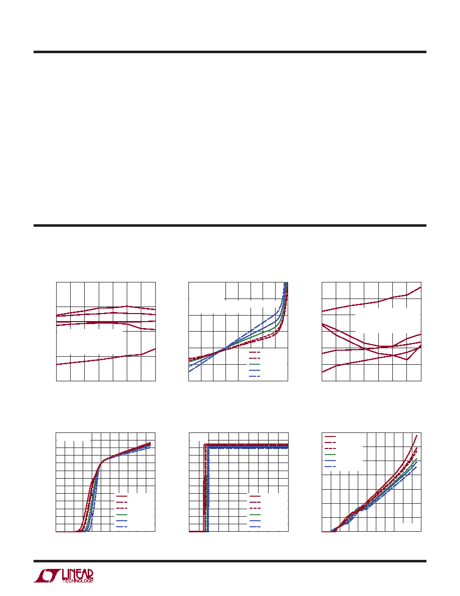
Supply Current vs Supply Voltage
Supply Current vs SHDN Voltage
Shutdown Supply Current vs
Supply Voltage
Differential Input Offset Voltage
vs Temperature
Differential Input Offset Voltage
vs Input Common Mode Voltage
Common Mode Offset Voltage
vs Temperature
elecTrical characTerisTics
Note 7: Input common mode range is tested by testing at both VICM = 1.25V
and at the Electrical Characteristics table limits to verify that the differential
offset (VOSDIFF) and the common mode offset (VOSCM) have not deviated by
more than ±1mV and ±2mV respectively from the VICM = 1.25V case.
The voltage range for the output common mode range is tested by
applying a voltage on the VOCM pin and testing at both VOCM = 1.25V and
at the Electrical Characteristics table limits to verify that the common
mode offset (VOSCM) has not deviated by more than ±6mV from the
VOCM = 1.25V case.
Note 8: Input CMRR is defined as the ratio of the change in the input
common mode voltage at the pins +IN or –IN to the change in differential
input referred offset voltage. Output CMRR is defined as the ratio of
the change in the voltage at the VOCM pin to the change in differential
input referred offset voltage. This specification is strongly dependent on
feedback ratio matching between the two outputs and their respective
inputs and it is difficult to measure actual amplifier performance (See
Effects of Resistor Pair Mismatch in the Applications Information section
of this data sheet). For a better indicator of actual amplifier performance
independent of feedback component matching, refer to the PSRR
specification.
Note 9: Differential power supply rejection (PSRR) is defined as the ratio
of the change in supply voltage to the change in differential input referred
offset voltage. Common mode power supply rejection (PSRRCM) is
defined as the ratio of the change in supply voltage to the change in the
output common mode offset voltage.
Note 10: Supply voltage range is guaranteed by power supply rejection
ratio test.
Note 11: Extended operation with the output shorted may cause the
junction temperature to exceed the 150°C limit.
Note 12: Refer to Relationship Between Different Linearity Metrics in the
Applications Information section of this data sheet for information on how
to calculate an equivalent OIP3 from IMD3 measurements.
TEMPERATURE (°C)
6409 G01
DIFFERENTIAL
V
OS
(mV)
VS = 5V
VOCM = VICM = 1.25V
RI = RF = 150
FIVE REPRESENTATIVE UNITS
–50
50
125
100
–25
0
25
75
1.5
1.0
0.5
0
–0.5
INPUT COMMON MODE VOLTAGE (V)
6409 G02
DIFFERENTIAL
V
OS
(mV)
VS = 5V
VOCM = 1.25V
RI = RF = 150
0.1% FEEDBACK NETWORK RESISTORS
REPRESENTATIVE UNIT
0
2
4
3
0.5
1
1.5
2.5
3.5
2.0
1.5
1.0
0.5
–0.5
0
–1.0
TA = 85°C
TA = 70°C
TA = 25°C
TA = 0°C
TA = –40°C
SUPPLY VOLTAGE (V)
6409 G04
TOT
AL
SUPPL
YCURRENT
(mA)
VSHDN = OPEN
0
2
5.5
3.5
3
0.5 1 1.5
2.5
4
5
4.5
60
20
15
25
30
35
40
45
50
55
10
5
0
TA = 125°C
TA = 85°C
TA = 70°C
TA = 25°C
TA = 0°C
TA = –40°C
SHDN VOLTAGE (V)
6409 G05
VS = 5V
TOT
AL
SUPPL
YCURRENT
(mA)
0
2
5
3.5
3
0.5 1 1.5
2.5
4 4.5
60
20
15
25
30
35
40
45
50
55
10
5
0
TA = 125°C
TA = 85°C
TA = 70°C
TA = 25°C
TA = 0°C
TA = –40°C
SUPPLY VOLTAGE (V)
6409 G06
SHUTDOWN
SUPPL
YCURRENT
(A)
VSHDN = V–
0
2
5.5
3.5
3
0.5 1 1.5
2.5
4
5
4.5
140
120
100
80
60
20
40
0
TA = 125°C
TA = 85°C
TA = 70°C
TA = 25°C
TA = 0°C
TA = –40°C
TEMPERATURE (°C)
6409 G03
COMMON
MODE
OFFSET
VOL
TAGE
(mV)
VS = 5V
VOCM = VICM = 1.25V
RI = RF = 150
FIVE REPRESENTATIVE UNITS
2.5
2.0
1.5
1.0
0.5
0
–0.5
–50
50
125
100
–25
0
25
75
相關(guān)PDF資料 |
PDF描述 |
|---|---|
| VE-B4F-MV-B1 | CONVERTER MOD DC/DC 72V 150W |
| SY88403BLEY TR | IC POST AMP CML TTL LOS 10-MSOP |
| AD5734RBREZ-REEL7 | IC DAC 14BIT DSP/SRL 24TSSOP |
| AD8138ARM-REEL7 | IC AMP DIFF LDIST LP 95MA 8MSOP |
| AD8138AR-REEL7 | IC AMP DIFF LDIST LP 95MA 8SOIC |
相關(guān)代理商/技術(shù)參數(shù) |
參數(shù)描述 |
|---|---|
| LTC6409HUDB#PBF | 制造商:Linear Technology 功能描述:DIFF-AMPLIFIER, 10GHZ, 3300V/US, QFN-10, No. of Amplifiers:1, Input Offset Voltage:300V, Bandwidth:10GHz, Amplifier Case Style:QFN, No. of Pins:10, Supply Voltage Range:2.7V to 5.25V, Slew Rate:3300V/s, Supply Current:52mA, MSL:- , RoHS Compliant: Yes |
| LTC6409HUDB#TRMPBF | 功能描述:IC AMP/DRIVER DIFF GBW 10-QFN RoHS:是 類別:集成電路 (IC) >> 線性 - 放大器 - 專用 系列:- 產(chǎn)品培訓(xùn)模塊:Lead (SnPb) Finish for COTS Obsolescence Mitigation Program 標(biāo)準(zhǔn)包裝:60 系列:- 類型:可變增益放大器 應(yīng)用:CATV 安裝類型:表面貼裝 封裝/外殼:20-WQFN 裸露焊盤 供應(yīng)商設(shè)備封裝:20-TQFN-EP(5x5) 包裝:托盤 |
| LTC6409HUDB#TRPBF | 功能描述:IC AMP/DRIVER DIFF GBW 10-QFN RoHS:是 類別:集成電路 (IC) >> 線性 - 放大器 - 專用 系列:- 產(chǎn)品培訓(xùn)模塊:Lead (SnPb) Finish for COTS Obsolescence Mitigation Program 標(biāo)準(zhǔn)包裝:60 系列:- 類型:可變增益放大器 應(yīng)用:CATV 安裝類型:表面貼裝 封裝/外殼:20-WQFN 裸露焊盤 供應(yīng)商設(shè)備封裝:20-TQFN-EP(5x5) 包裝:托盤 |
| LTC6409HUDBTRMPBF | 制造商:LINER 制造商全稱:Linear Technology 功能描述:10GHz GBW, 1.1nV/Hz Differential Amplifier/ADC Driver |
| LTC6409IUDB#PBF | 制造商:Linear Technology 功能描述:SP Amp DIFF AMP Single 5.25V 10-Pin QFN EP 制造商:Linear Technology 功能描述:Bulk |
發(fā)布緊急采購,3分鐘左右您將得到回復(fù)。