- 您現(xiàn)在的位置:買賣IC網(wǎng) > PDF目錄367613 > LUCL9215GRG-D Short-Loop Sine Wave Ringing SLIC PDF資料下載
參數(shù)資料
| 型號: | LUCL9215GRG-D |
| 英文描述: | Short-Loop Sine Wave Ringing SLIC |
| 中文描述: | 短回路正弦波振鈴用戶接口 |
| 文件頁數(shù): | 27/50頁 |
| 文件大小: | 1115K |
| 代理商: | LUCL9215GRG-D |
第1頁第2頁第3頁第4頁第5頁第6頁第7頁第8頁第9頁第10頁第11頁第12頁第13頁第14頁第15頁第16頁第17頁第18頁第19頁第20頁第21頁第22頁第23頁第24頁第25頁第26頁當(dāng)前第27頁第28頁第29頁第30頁第31頁第32頁第33頁第34頁第35頁第36頁第37頁第38頁第39頁第40頁第41頁第42頁第43頁第44頁第45頁第46頁第47頁第48頁第49頁第50頁

Data Sheet
September 2001
Short-Loop Sine Wave Ringing SLIC
L9215A/G
Agere Systems Inc.
27
Supervision
The L9215 offers the loop closure and ring trip supervi-
sion functions. Internal to the device, the outputs of
these detectors are multiplexed into a single package
output, NSTAT. Additionally, a common-mode current
detector for tip or ring ground detection is included for
ground key applications.
Loop Closure
The loop closure has a fixed typical 10.5 mA on- to off-
hook threshold in the active mode and a fixed 11.5 mA
on- to off-hook threshold from the scan mode. In either
case, there is a 2 mA hysteresis with V
CC
= 5 V and a
1 mA hysteresis with V
CC
= 3.3 V.
Ring Trip
The ring trip detector requires only a single-pole filter at
the input, minimizing external components. An R/C
combination of 383 k
and 0.1
μ
F, for a filter pole at
5.15 Hz, is recommended.
The ring trip threshold is internally fixed as a function of
battery voltage and is given by:
RT (mA) = 67 * {(0.0045 * V
BAT1
) + 0.317}
where:
RT is ring trip current in mA.
V
BAT1
is the magnitude of the ring battery in V.
There is a 6 mA to 8 mA hysteresis.
Tip or Ring Ground Detector
In the ground key or ground start applications, a com-
mon-mode current detector is used to indicate either a
tip- or ring-ground has occurred (ground key) or an off-
hook has occurred (ground start). The detection thresh-
old is set by connecting a resistor from ICM to V
CC
.
170 x V
CC
/R
ICM
(k
) = I
TH
(mA)
Additionally, a filter capacitor across R
ICM
will set the
time constant of the detector. No hysteresis is associ-
ated with this detector.
Power Ring
The device offers a ring mode, in which a balanced
power ring signal is provided to the tip/ring pair. During
the ring mode, a user-supplied low-voltage ring signal
is input to the device’s RING
IN
input. This signal is
amplified to produce the balanced power ring signal.
The user may supply a sine wave input, PWM input, or
a square wave to produce sinusoidal or trapezoidal
ringing at tip and ring.
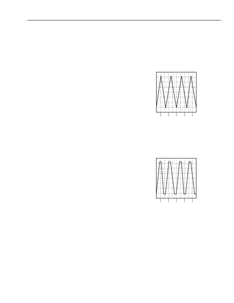
Various crest factors are shown below for illustrative
purposes.
12-3346a (F)
Note: Slew rate = 5.65 V/ms; trise = tfall = 23 ms; pwidth = 2 ms;
period = 50 ms.
Figure 9. Ringing Waveform Crest Factor = 1.6
12-3347a (F)
Note: Slew rate = 10.83 V/ms; trise = tfall = 12 ms; pwidth = 13 ms;
period = 50 ms.
Figure 10. Ringing Waveform Crest Factor = 1.2
Voltage applied to the load may be increased by using
a filtered square wave input to produce a lower crest
factor trapezoidal power ring signal at tip and ring.
TIME (s)
–80
–60
–40
–20
0
20
40
60
80
0.00
0.02 0.06
0.04 0.08
0.10
0.12
0.14
0.16
0.18
0.20
V
TIME (s)
–80
–60
–40
–20
0
20
40
60
80
0.00
0.02 0.06
0.04 0.08
0.10
0.12
0.14
0.16
0.18
0.20
V
相關(guān)PDF資料 |
PDF描述 |
|---|---|
| LUCL9215GAU-D | Short-Loop Sine Wave Ringing SLIC |
| LUCL9215ARG-D | Short-Loop Sine Wave Ringing SLIC |
| LUCL9215AAU-D | GT 3C 3#0 PIN RECP WALL RM |
| LUCL9215AAU-DT | GT 14C 12# 2#16 PIN RECP WALL |
| LUCL9216GGF-D | Short-Loop Ringing SLIC with Ground Start |
相關(guān)代理商/技術(shù)參數(shù) |
參數(shù)描述 |
|---|---|
| LUCL9216AGF-D | 制造商:AGERE 制造商全稱:AGERE 功能描述:Short-Loop Ringing SLIC with Ground Start |
| LUCL9216AGF-DT | 制造商:AGERE 制造商全稱:AGERE 功能描述:Short-Loop Ringing SLIC with Ground Start |
| LUCL9216ARG-D | 制造商:AGERE 制造商全稱:AGERE 功能描述:Short-Loop Ringing SLIC with Ground Start |
| LUCL9216GGF-D | 制造商:AGERE 制造商全稱:AGERE 功能描述:Short-Loop Ringing SLIC with Ground Start |
| LUCL9216GGF-DT | 制造商:AGERE 制造商全稱:AGERE 功能描述:Short-Loop Ringing SLIC with Ground Start |
發(fā)布緊急采購,3分鐘左右您將得到回復(fù)。