- 您現(xiàn)在的位置:買賣IC網(wǎng) > PDF目錄358093 > M2006-01-669.1281LF (INTEGRATED DEVICE TECHNOLOGY INC) ATM/SONET/SDH SUPPORT CIRCUIT, QCC36 PDF資料下載
參數(shù)資料
| 型號: | M2006-01-669.1281LF |
| 廠商: | INTEGRATED DEVICE TECHNOLOGY INC |
| 元件分類: | 數(shù)字傳輸電路 |
| 英文描述: | ATM/SONET/SDH SUPPORT CIRCUIT, QCC36 |
| 封裝: | 9 X 9 MM, SMT-36 |
| 文件頁數(shù): | 2/10頁 |
| 文件大小: | 911K |
| 代理商: | M2006-01-669.1281LF |

Micro Networks 324 Clark Street Worcester, MA 01606 tel: 508-852-5400 fax: 508-852-8456 www.micronetworks.com
2
M2006-01
Prelimnary Specifications
Micro Networks
An Integrated Circuit Systems Company
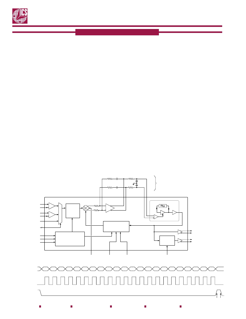
FUNCTIONAL BLOCK DIAGRAM
The internal PLL will adjust the VCSO output
frequency to be M (feedback divider) divided by R
(input divider) times the selected input reference clock
frequency. Note that the ratio of M/R times input
frequency must be such that it falls within the “l(fā)ock”
range of the VCSO. The M divider (10-bits) can be
programmed for a maximum value of 1023 and a
minimum value of 4. The R divider (9-bits) can be set
to a maximum value of 511 and a minimum value of 1.
There are two differential LVPECL outputs (Fout 0,
Fout 1) which operate at the VCSO frequency. When
P1 is HIGH the Fout 1 output will operate at 1/4 the
VCSO frequency and when P1 is LOW Fout 1 output
operates at the VCSO frequency.
The relationship between the VCSO frequency, the M
and R dividers, and the input REF_CLK is defined as
follows:
F VCSO = F REF_CLK x M / R
On power-up the R and M dividers are set to 1 and
32, respectively.
The input reference clock is selected from DIF_CLK 0,
DIF_CLK 1, or REF_CLK by selecting the appropriate
REF_SEL 0 and REF_SEL 1 inputs. When a new
reference is selected the M2006-01 will automatically
switch to the “phase slope limiting” mode to control
the phase build-out of the output clocks.
The ADD_CLK and DROP_CLK inputs increments or
decrements the M (feedback) divider for one phase
detector cycle. This results in a momentary increase or
decrease in output frequency and an extra or missing
output clock cycle relative to the input reference clock.
The "phase slope limiter" is used to ensure MTIE
compliance. The PSL input provides manual control.
When PSL is HIGH, the output phase slope is limited by
changing the phase detector gain to a non-linear function.
The M2006-01 is serially programmed via a 3 wire interface.
.
Refer to the timing diagram below (labeled "SERIAL
PROGRAMMING") for the following explanation.
Serial operation begins at point "(a)", when S_LOAD is LOW;
the shift register is loaded one bit at-a-time by sampling
the S_DATA bits with the rising edge of S_CLOCK.
Divider load
occurs at point "(b)" , when S_LOAD transitions
from LOW to HIGH; all of the data in the shift register is
loaded into the R and M dividers.
Latch
occurs at point "(c)", on the HIGH-to-LOW transition of
S_LOAD; divider values will not be affected by serial input.
(If S_LOAD is held HIGH, any S_DATA input is passed directly
to the R and M dividers on each rising edge of S_CLOCK.)
Note: T1 andT0, whchare usedfor test automation must be set to0. T2 is set to1 for normal bandwidth 0 for narrow bandwidth
S_DATA
T2
T1
T0
R8
R7
R6
R5
R4
R3
R2
R1
R0
M9
M8
M7
M6
M5
M4
M3
M2
M1
M0
S_CLOCK
S_LOAD
SERIAL PROGRAMMING
M2006-01
SAW Delay Line
Phase
Shifter
VCSO
C
POST
C
POST
VC
nVC
R
POST
nOP_OUT
OP_OUT
R
POST
R
LOOP
R
LOOP
C
LOOP
C
LOOP
R
IN
R
IN
OP_IN
nOP_IN
M Divider
M = 3-1024
Power-Up Default = 32
Serial
Configuration
Register
Phase
Detector
Loop Filter
Amplifier
External
Loop Filter
Components
FOUT0
nFOUT0
S_DATA
S_CL
OC
K
S_LOAD
R Divider
R = 1-511
Power-Up
Default = 1
MUX
00
REF_SEL1:0
REF_CLK
DIF_REF1
nDIF_REF1
DIF_REF0
nDIF_REF0
01
1X
2
ADD_CLK
DROP_CLK
P Divider
P = 1 ( P1 = 0 )
or 4 ( P1 = 1 )
FOUT1
nFOUT1
P1
PSL
(a)
(b) (c)
相關PDF資料 |
PDF描述 |
|---|---|
| M2006-01-669.1281 | ATM/SONET/SDH SUPPORT CIRCUIT, QCC36 |
| M2006-01-669.3266LF | ATM/SONET/SDH SUPPORT CIRCUIT, QCC36 |
| M2006-01-669.3266 | ATM/SONET/SDH SUPPORT CIRCUIT, QCC36 |
| M2006-01-672.1600LF | ATM/SONET/SDH SUPPORT CIRCUIT, QCC36 |
| M2006-01-672.1600 | ATM/SONET/SDH SUPPORT CIRCUIT, QCC36 |
相關代理商/技術參數(shù) |
參數(shù)描述 |
|---|---|
| M2006-02 | 制造商:ICS 制造商全稱:ICS 功能描述:VCSO BASED FEC CLOCK PLL / HITLESS SWITCHING OPTION |
| M2006-02-622.08 | 制造商:Integrated Device Technology Inc 功能描述:M2006-02-622.08 - Bulk |
| M2006-02-622.0800 | 功能描述:時鐘合成器/抖動清除器 FREQUENCY TRANSLATOR RoHS:否 制造商:Skyworks Solutions, Inc. 輸出端數(shù)量: 輸出電平: 最大輸出頻率: 輸入電平: 最大輸入頻率:6.1 GHz 電源電壓-最大:3.3 V 電源電壓-最小:2.7 V 封裝 / 箱體:TSSOP-28 封裝:Reel |
| M2006-02-622.0800T | 功能描述:時鐘合成器/抖動清除器 FREQUENCY TRANSLATOR RoHS:否 制造商:Skyworks Solutions, Inc. 輸出端數(shù)量: 輸出電平: 最大輸出頻率: 輸入電平: 最大輸入頻率:6.1 GHz 電源電壓-最大:3.3 V 電源電壓-最小:2.7 V 封裝 / 箱體:TSSOP-28 封裝:Reel |
| M2006-02-625.0000 | 制造商:Integrated Device Technology Inc 功能描述:PLL Clock Generator Single 625MHz 36-Pin CLCC 制造商:Integrated Device Technology Inc 功能描述:9X9 LCC(LEAD FREE) - Bulk 制造商:Integrated Device Technology Inc 功能描述:FREQUENCY TRANSLATOR |
發(fā)布緊急采購,3分鐘左右您將得到回復。