- 您現(xiàn)在的位置:買賣IC網 > PDF目錄358093 > M2006-01-669.3266 (INTEGRATED DEVICE TECHNOLOGY INC) ATM/SONET/SDH SUPPORT CIRCUIT, QCC36 PDF資料下載
參數資料
| 型號: | M2006-01-669.3266 |
| 廠商: | INTEGRATED DEVICE TECHNOLOGY INC |
| 元件分類: | 數字傳輸電路 |
| 英文描述: | ATM/SONET/SDH SUPPORT CIRCUIT, QCC36 |
| 封裝: | 9 X 9 MM, SMT-36 |
| 文件頁數: | 1/10頁 |
| 文件大?。?/td> | 911K |
| 代理商: | M2006-01-669.3266 |

Micro Networks 324 Clark Street Worcester, MA 01606 tel: 508-852-5400 fax: 508-852-8456 www.micronetworks.com
1
M2006-01
Prelimnary Specifications
Micro Networks
An Integrated Circuit Systems Company
Registered
ISO 9001
M2006-01
Frequency Synthesizer
APPLICATIONS
SONET / SDH / 10GbE System
Synchronization
Add / Drop Muxes, Access and Edge
Switches
Line Card System Clock Cleaner /
Translator
Optical Module Clock Cleaner / Translator
DESCRIPTION
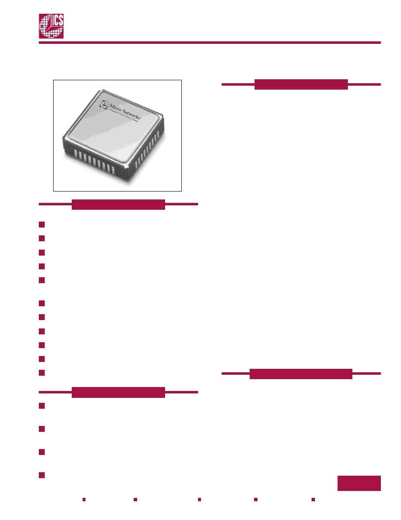
The M2006-01 integrates a high performance Phase Locked
Loop (PLL) with a Voltage Controlled SAW Oscillator (VCSO)
to provide a low jitter Frequency Synthesizer in a 9mm x
9mm surface mount package.
The internal high “Q” SAW filter provides low jitter signal
performance and determines the output frequency of the
VCSO.
Selecting between two differential LVPECL clocks or one
single-ended LVCMOS / LVTTL clock provides the input
reference signal to the Frequency Translator. The maximum
input frequency is 700MHz.
The M2006-01 will default to a multiplying factor of 32 on
power-up. The multiplying factor can be changed by serially
programming the input and feedback dividers via the
configuration logic.
A differential LVPECL signal provides the output clock for
the device. A second differential output which can be
programmed to divide the output frequency by a factor of 4
is also available. The output frequency can be momentarily
increased or decreased to add or subtract one net output
clock cycle by asserting the ADD_CLK or DROP_CLK
inputs, respectively.
An external loop filter sets the PLL bandwidth which can be
optimized to provide jitter attenuation of the input reference
clock. A phase slope limiting feature, which reduces phase
build-out in order to meet GR-253 MTIE upon an input
transient, can be manually selected by asserting the PSL
input. The phase slope limiting feature is automatically
activated whenever a new input reference clock is selected.
The frequency agility, bandwidth control, and phase slope
limiting features make the M2006-01 ideal for use as a clock
jitter attenuator, frequency translator, and clock frequency
generator in OC-3 through OC-192 applications.
Inputs, V
I
:
Output, V
O
:
Supply Voltage, V
CC
: ......................................................... 4.6 V
Storage Temperature, T
STO
:............................ -45
°
C to +100
°
C
................................................. -0.5 to V
CC
+0.5V
................................................. -0.5 to V
CC
+0.5V
ABSOLUTE MAX RATINGS
Output Clock Frequency up to 700MHz
Intrinsic Jitter <1ps rms (12kHz - 50MHz)
Automatic Phase Slope Limiting
Dual Differential Inputs
Input Compatible with LVPECL, LVDS,
HSTL, SSTL, etc.
Triple Input MUX
Configurable Input and Feedback Dividers
Tunable Loop Filter Response
Two Differential LVPECL outputs
Single 3.3V Supply
Small 9mm x 9mm SMT Package
FEATURES
Stresses beyondthose listedunder Absoute MaximumRatings may cause
permanent damage tothe device. These ratings are stress specifications ony
Functional operationof product at these condtions or any condtions beyond
those listedinthe DC Characteristics or AC Characteristics is not impied
Exposure toabsoute maximumrating condtions for extendedperiods may
affect product reliablity
相關PDF資料 |
PDF描述 |
|---|---|
| M2006-01-672.1600LF | ATM/SONET/SDH SUPPORT CIRCUIT, QCC36 |
| M2006-01-672.1600 | ATM/SONET/SDH SUPPORT CIRCUIT, QCC36 |
| M2006-01-690.5692LF | ATM/SONET/SDH SUPPORT CIRCUIT, QCC36 |
| M2006-01-690.5692 | ATM/SONET/SDH SUPPORT CIRCUIT, QCC36 |
| M2006-01-693.4830LF | ATM/SONET/SDH SUPPORT CIRCUIT, QCC36 |
相關代理商/技術參數 |
參數描述 |
|---|---|
| M2006-02 | 制造商:ICS 制造商全稱:ICS 功能描述:VCSO BASED FEC CLOCK PLL / HITLESS SWITCHING OPTION |
| M2006-02-622.08 | 制造商:Integrated Device Technology Inc 功能描述:M2006-02-622.08 - Bulk |
| M2006-02-622.0800 | 功能描述:時鐘合成器/抖動清除器 FREQUENCY TRANSLATOR RoHS:否 制造商:Skyworks Solutions, Inc. 輸出端數量: 輸出電平: 最大輸出頻率: 輸入電平: 最大輸入頻率:6.1 GHz 電源電壓-最大:3.3 V 電源電壓-最小:2.7 V 封裝 / 箱體:TSSOP-28 封裝:Reel |
| M2006-02-622.0800T | 功能描述:時鐘合成器/抖動清除器 FREQUENCY TRANSLATOR RoHS:否 制造商:Skyworks Solutions, Inc. 輸出端數量: 輸出電平: 最大輸出頻率: 輸入電平: 最大輸入頻率:6.1 GHz 電源電壓-最大:3.3 V 電源電壓-最小:2.7 V 封裝 / 箱體:TSSOP-28 封裝:Reel |
| M2006-02-625.0000 | 制造商:Integrated Device Technology Inc 功能描述:PLL Clock Generator Single 625MHz 36-Pin CLCC 制造商:Integrated Device Technology Inc 功能描述:9X9 LCC(LEAD FREE) - Bulk 制造商:Integrated Device Technology Inc 功能描述:FREQUENCY TRANSLATOR |
發(fā)布緊急采購,3分鐘左右您將得到回復。