- 您現(xiàn)在的位置:買賣IC網(wǎng) > PDF目錄45033 > M37516E6HP 8-BIT, OTPROM, 4 MHz, MICROCONTROLLER, PQFP48 PDF資料下載
參數(shù)資料
| 型號: | M37516E6HP |
| 元件分類: | 微控制器/微處理器 |
| 英文描述: | 8-BIT, OTPROM, 4 MHz, MICROCONTROLLER, PQFP48 |
| 封裝: | 7 X 7 MM, 0.50 MM PITCH, PLASTIC, LQFP-48 |
| 文件頁數(shù): | 44/90頁 |
| 文件大小: | 1144K |
| 代理商: | M37516E6HP |
第1頁第2頁第3頁第4頁第5頁第6頁第7頁第8頁第9頁第10頁第11頁第12頁第13頁第14頁第15頁第16頁第17頁第18頁第19頁第20頁第21頁第22頁第23頁第24頁第25頁第26頁第27頁第28頁第29頁第30頁第31頁第32頁第33頁第34頁第35頁第36頁第37頁第38頁第39頁第40頁第41頁第42頁第43頁當(dāng)前第44頁第45頁第46頁第47頁第48頁第49頁第50頁第51頁第52頁第53頁第54頁第55頁第56頁第57頁第58頁第59頁第60頁第61頁第62頁第63頁第64頁第65頁第66頁第67頁第68頁第69頁第70頁第71頁第72頁第73頁第74頁第75頁第76頁第77頁第78頁第79頁第80頁第81頁第82頁第83頁第84頁第85頁第86頁第87頁第88頁第89頁第90頁
Rev.1.01
Jul 01, 2003
page 49 of 89
7516 Group
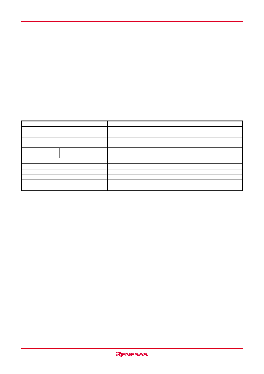
Table 13 Summary of M37516F8 (flash memory version)
FLASH MEMORY MODE
The M37516F8 (flash memory version) has an internal new
DINOR (DIvided bit line NOR) flash memory that can be rewritten
with a single power source when VCC is 5 V, and 2 power sources
when VPP is 5 V and VCC is 3.0-5.5 V in the CPU rewrite and stan-
dard serial I/O modes.
For this flash memory, three flash memory modes are available in
which to read, program, and erase: the parallel I/O and standard
serial I/O modes in which the flash memory can be manipulated
using a programmer and the CPU rewrite mode in which the flash
memory can be manipulated by the Central Processing Unit
(CPU).
Summary
Table 13 lists the summary of the M37516F8 (flash memory ver-
sion).
The flash memory of the M37516F8 is divided into User ROM area
and Boot ROM area as shown in Figure 57.
In addition to the ordinary User ROM area to store the MCU op-
eration control program, the flash memory has a Boot ROM area
that is used to store a program to control rewriting in CPU rewrite
and standard serial I/O modes. This Boot ROM area has had a
standard serial I/O mode control program stored in it when
shipped from the factory. However, the user can write a rewrite
control program in this area that suits the user’s application sys-
tem. This Boot ROM area can be rewritten in only parallel I/O
mode.
Item
Power source voltage
VPP voltage (For Program/Erase)
Flash memory mode
Erase block division
User ROM area
Boot ROM area
Program method
Erase method
Program/Erase control method
Number of commands
Number of program/Erase times
ROM code protection
Specifications
Vcc = 2.7– 5.5 V (Note 1)
Vcc = 2.7–3.6 V (Note 2)
4.5-5.5 V, f(XIN) = 8 MHz
3 modes (Parallel I/O mode, Standard serial I/O mode, CPU rewrite mode)
1 block (32 Kbytes)
1 block (4 Kbytes) (Note 3)
Byte program
Batch erasing
Program/Erase control by software command
6 commands
100 times
Available in parallel I/O mode and standard serial I/O mode
Notes 1: The power source voltage must be Vcc = 4.5–5.5 V at program and erase operation.
2: The power source voltage can be Vcc = 3.0–3.6 V also at program and erase operation.
3: The Boot ROM area has had a standard serial I/O mode control program stored in it when shipped from the factory. This Boot ROM area can be
rewritten in only parallel I/O mode.
相關(guān)PDF資料 |
PDF描述 |
|---|---|
| M37516M8-XXXHP | 8-BIT, MROM, 4 MHz, MICROCONTROLLER, PQFP48 |
| M37516M4H-XXXKP | 8-BIT, MROM, 4 MHz, MICROCONTROLLER, PQFP44 |
| M37516M6H-XXXKP | 8-BIT, MROM, 4 MHz, MICROCONTROLLER, PQFP44 |
| M37517F8HP | 8-BIT, FLASH, 4 MHz, MICROCONTROLLER, PQFP48 |
| M37524E4-XXXSP | 8-BIT, OTPROM, 4 MHz, MICROCONTROLLER, PDIP64 |
相關(guān)代理商/技術(shù)參數(shù) |
參數(shù)描述 |
|---|---|
| M37516E6H-XXXKP | 制造商:RENESAS 制造商全稱:Renesas Technology Corp 功能描述:SINGLE-CHIP 8-BIT CMOS MICROCOMPUTER |
| M37516E6-XXXHP | 制造商:RENESAS 制造商全稱:Renesas Technology Corp 功能描述:SINGLE-CHIP 8-BIT CMOS MICROCOMPUTER |
| M37516E6-XXXKP | 制造商:RENESAS 制造商全稱:Renesas Technology Corp 功能描述:SINGLE-CHIP 8-BIT CMOS MICROCOMPUTER |
| M37516E7H-XXXKP | 制造商:RENESAS 制造商全稱:Renesas Technology Corp 功能描述:SINGLE-CHIP 8-BIT CMOS MICROCOMPUTER |
| M37516E7-XXXHP | 制造商:RENESAS 制造商全稱:Renesas Technology Corp 功能描述:SINGLE-CHIP 8-BIT CMOS MICROCOMPUTER |
發(fā)布緊急采購,3分鐘左右您將得到回復(fù)。