- 您現(xiàn)在的位置:買賣IC網(wǎng) > PDF目錄370953 > M3850B1 (Mitsubishi Electric Corporation) SINGLE-CHIP 8-BIT CMOS MICROCOMPUTER PDF資料下載
參數(shù)資料
| 型號(hào): | M3850B1 |
| 廠商: | Mitsubishi Electric Corporation |
| 英文描述: | SINGLE-CHIP 8-BIT CMOS MICROCOMPUTER |
| 中文描述: | 單芯片8位CMOS微機(jī) |
| 文件頁(yè)數(shù): | 18/52頁(yè) |
| 文件大?。?/td> | 807K |
| 代理商: | M3850B1 |
第1頁(yè)第2頁(yè)第3頁(yè)第4頁(yè)第5頁(yè)第6頁(yè)第7頁(yè)第8頁(yè)第9頁(yè)第10頁(yè)第11頁(yè)第12頁(yè)第13頁(yè)第14頁(yè)第15頁(yè)第16頁(yè)第17頁(yè)當(dāng)前第18頁(yè)第19頁(yè)第20頁(yè)第21頁(yè)第22頁(yè)第23頁(yè)第24頁(yè)第25頁(yè)第26頁(yè)第27頁(yè)第28頁(yè)第29頁(yè)第30頁(yè)第31頁(yè)第32頁(yè)第33頁(yè)第34頁(yè)第35頁(yè)第36頁(yè)第37頁(yè)第38頁(yè)第39頁(yè)第40頁(yè)第41頁(yè)第42頁(yè)第43頁(yè)第44頁(yè)第45頁(yè)第46頁(yè)第47頁(yè)第48頁(yè)第49頁(yè)第50頁(yè)第51頁(yè)第52頁(yè)
18
3850 Group
SINGLE-CHIP 8-BIT CMOS MICROCOMPUTER
MITSUBISHI MICROCOMPUTERS
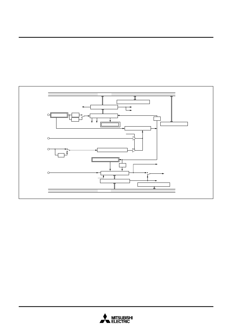
(2) Asynchronous Serial I/O (UART) Mode
Clock asynchronous serial I/O mode (UART) can be selected by
clearing the serial I/O mode selection bit (b6) of the serial I/O con-
trol register to “0”.
Eight serial data transfer formats can be selected, and the transfer
formats used by a transmitter and receiver must be identical.
The transmit and receive shift registers each have a buffer, but the
two buffers have the same address in memory. Since the shift reg-
ister cannot be written to or read from directly, transmit data is
written to the transmit buffer register, and receive data is read from
the receive buffer register.
The transmit buffer register can also hold the next data to be
transmitted, and the receive buffer register can hold a character
while the next character is being received.
Fig.17 Block diagram of UART serial I/O
X
IN
1/4
OE
PE FE
1/16
1/16
Data bus
Receive buffer register
Address 0018
16
Receive shift register
Receive buffer full flag (RBF)
Receive interrupt request (RI)
Baud rate generator
Address 001C
16
Frequency division ratio 1/(n+1)
ST/SP/PA generator
Transmit buffer register
Data bus
Transmit shift register
Address
0018
16
Transmit shift completion flag (TSC)
Transmit buffer empty flag (TBE)
Address
0019
16
Serial I/O status register
Transmit interrupt request (TI)
ST detector
SP detector
UART control register
Address 001B
16
Character length selection bit
Address 001A
16
BRG count source selection bit
Transmit interrupt source selection bit
Serial I/O synchronous clock selection bit
Clock control circuit
Character length selection bit
7 bits
8 bits
Serial I/O control register
P2
6
/S
CLK1
P2
4
/R
X
D
P2
5
/T
X
D
相關(guān)PDF資料 |
PDF描述 |
|---|---|
| M38503E4-081FP | SINGLE-CHIP 8-BIT CMOS MICROCOMPUTER |
| M38503M4-067FP | SINGLE-CHIP 8-BIT CMOS MICROCOMPUTER |
| M38503M4-094FP | SINGLE-CHIP 8-BIT CMOS MICROCOMPUTER |
| M38504M6-200FP | SINGLE-CHIP 8-BIT CMOS MICROCOMPUTER |
| M38504M6-201FP | SINGLE-CHIP 8-BIT CMOS MICROCOMPUTER |
相關(guān)代理商/技術(shù)參數(shù) |
參數(shù)描述 |
|---|---|
| M3851 BK001 | 制造商:Alpha Wire Company 功能描述:CBL 7COND 14AWG BLK 1000' |
| M3851 BK002 | 制造商:Alpha Wire Company 功能描述:CBL 7COND 14AWG BLK 500' |
| M3851 BK005 | 制造商:Alpha Wire Company 功能描述:CBL 7COND 14AWG BLK 100' |
| M38510/00102BCB | 制造商:n/a 功能描述:38510/00102 S6I6B 制造商: 功能描述: 制造商:undefined 功能描述: |
| M38510/00103BCA | 制造商:QP Semiconductor 功能描述:NAND GATE, TRIPLE 3-INPUT |
發(fā)布緊急采購(gòu),3分鐘左右您將得到回復(fù)。