- 您現(xiàn)在的位置:買賣IC網(wǎng) > PDF目錄45048 > M38C89EFFP 8-BIT, OTPROM, 4 MHz, MICROCONTROLLER, PQFP144 PDF資料下載
參數(shù)資料
| 型號(hào): | M38C89EFFP |
| 元件分類: | 微控制器/微處理器 |
| 英文描述: | 8-BIT, OTPROM, 4 MHz, MICROCONTROLLER, PQFP144 |
| 封裝: | 20 X 20 MM, 0.50 MM PITCH, PLASTIC, LQFP-144 |
| 文件頁數(shù): | 40/55頁 |
| 文件大?。?/td> | 981K |
| 代理商: | M38C89EFFP |
第1頁第2頁第3頁第4頁第5頁第6頁第7頁第8頁第9頁第10頁第11頁第12頁第13頁第14頁第15頁第16頁第17頁第18頁第19頁第20頁第21頁第22頁第23頁第24頁第25頁第26頁第27頁第28頁第29頁第30頁第31頁第32頁第33頁第34頁第35頁第36頁第37頁第38頁第39頁當(dāng)前第40頁第41頁第42頁第43頁第44頁第45頁第46頁第47頁第48頁第49頁第50頁第51頁第52頁第53頁第54頁第55頁
44
SINGLE-CHIP 8-BIT CMOS MICROCOMPUTER
MITSUBISHI MICROCOMPUTERS
38C8 Group
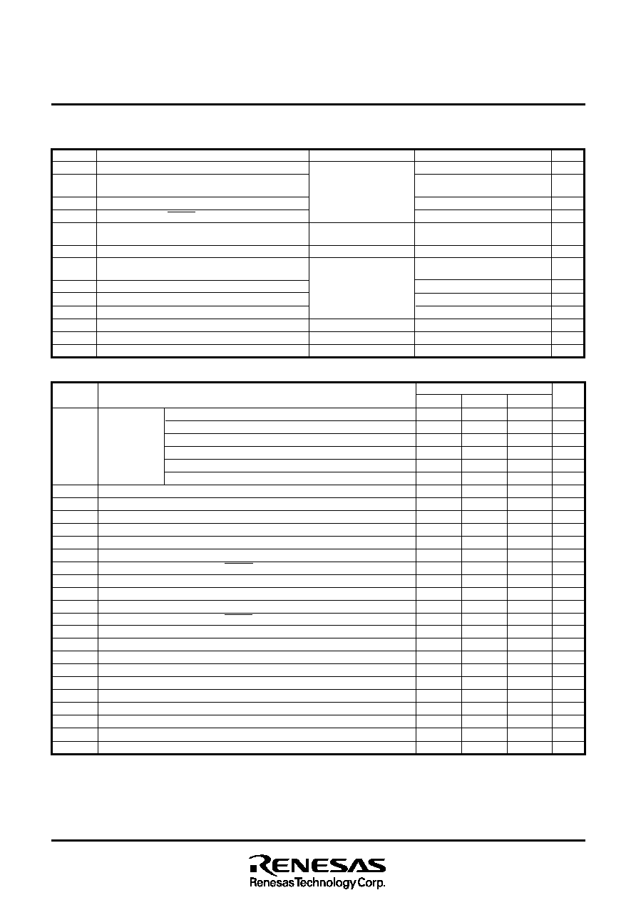
Parameter
Power source voltage
Input voltage
P00–P07, P10–P17, P20–P27,
P30–P33, P40–P47
Input voltage
C1, C2
Input voltage
RESET, XIN, XCIN
Input voltage
VLIN
Input voltage
VL1, VL2, VL3, VL4, VL5
Output voltage
P00–P07, P10–P17, P20–P27,
P30–P33, P41–P47
Output voltage
C1, C2, C3
Output voltage
COM0–COM31, SEG0–SEG67
Output voltage
XOUT, XCOUT
Power dissipation
Operating temperature
Storage temperature
Symbol
VCC
VI
VO
Pd
Topr
Tstg
ELECTRICAL CHARACTERISTICS
Table 11 Absolute maximum ratings
Conditions
Ratings
–0.3 to 7.0
–0.3 to VCC+0.3
–0.3 to 7.0
–0.3 to VCC+0.3
–0.3 to 7.0
–0.3 to VCC+0.3
–0.3 to 7.0
–0.3 to VL5+0.3
–0.3 to VCC+0.3
300
–20 to 85
–40 to 125
Unit
V
mW
°C
All voltages are based on
Vss. Output transistors
are cut off.
When voltage multiplier is
not operated.
VL1
≤VL2≤VL3≤VL4≤VL5
Ta = 25°C
Table 12 Recommended operating conditions (Vcc = 2.2 to 5.5 V, Ta = –20 to 85°C, unless otherwise noted)
Power source
High-speed mode f(XIN)
≤ 8 MHz
voltage
Middle-speed mode f(XIN)
≤ 8 MHz
Middle-speed mode (mask ROM version) f(XIN)
≤ 4 MHz
Middle-speed mode (One Time PROM version) f(XIN)
≤ 4 MHz
Low-speed mode (mask ROM version)
Low-speed mode (One Time PROM version)
Power source voltage
VLIN
Power source voltage
VL5
Analog input voltage
AIN0–AIN7
“H” input voltage
P00–P07, P10–P17, P45, P47
“H” input voltage
P20–P27, P30–P33, P40–P43, P44, P46
“H” input voltage
RESET
“H” input voltage
XIN
“L” input voltage
P00–P07, P10–P17, P45, P47
“L” input voltage
P20–P27, P30–P33, P40–P43, P44, P46
“L” input voltage
RESET
“L” input voltage
XIN
“H” total peak output current
All ports
(Note 1)
“L” total peak output current
All ports
(Note 1)
“H” total average output current All ports
(Note 2)
“L” total average output current All ports
(Note 2)
“H” peak output current
All ports
(Note 3)
“L” peak output current
All ports
(Note 3)
“H” average output current
All ports
(Note 4)
“L” average output current
All ports
(Note 4)
Oscillation resistor at selecting RC oscillation
VCC
VSS
VLIN
VL5
VIA
VIH
VIL
ΣIOH(peak)
ΣIOL(peak)
ΣIOH(avg)
ΣIOL(avg)
IOH(peak)
IOL(peak)
IOH(avg)
IOL(avg)
ROSC
Limits
V
mA
k
Parameter
Min.
4.0
2.7
2.2
2.5
2.2
2.5
VSS
0.7VCC
0.8VCC
VSS
5
Typ.
5.0
0
8.2
Max.
5.5
2.33
7.0
VCC
0.3VCC
0.2VCC
–60.0
60.0
–30.0
30.0
–5.0
10.0
–2.5
5.0
10
Symbol
Unit
Notes 1: The total peak output current is the peak value of the peak currents flowing through all the applicable ports.
2: The total average output current is the average value measured over 100 ms flowing through all the applicable ports.
3: The peak output current is the peak current flowing in each port.
4: The average output current is an average value measured over 100 ms.
相關(guān)PDF資料 |
PDF描述 |
|---|---|
| M38C89MF-XXXFP | 8-BIT, MROM, 4 MHz, MICROCONTROLLER, PQFP144 |
| M38C89EFFP | 8-BIT, OTPROM, 4 MHz, MICROCONTROLLER, PQFP144 |
| M38D24G6HP | 8-BIT, FLASH, 6.25 MHz, MICROCONTROLLER, PQFP64 |
| M38D24G4FP | 8-BIT, FLASH, 6.25 MHz, MICROCONTROLLER, PQFP64 |
| M38D24G4-XXXHP | 8-BIT, FLASH, 6.25 MHz, MICROCONTROLLER, PQFP64 |
相關(guān)代理商/技術(shù)參數(shù) |
參數(shù)描述 |
|---|---|
| M38D20F1XXXFP | 制造商:RENESAS 制造商全稱:Renesas Technology Corp 功能描述:SINGLE-CHIP 8-BIT CMOS MICROCOMPUTER |
| M38D20F1XXXHP | 制造商:RENESAS 制造商全稱:Renesas Technology Corp 功能描述:SINGLE-CHIP 8-BIT CMOS MICROCOMPUTER |
| M38D20F2XXXFP | 制造商:RENESAS 制造商全稱:Renesas Technology Corp 功能描述:SINGLE-CHIP 8-BIT CMOS MICROCOMPUTER |
| M38D20F2XXXHP | 制造商:RENESAS 制造商全稱:Renesas Technology Corp 功能描述:SINGLE-CHIP 8-BIT CMOS MICROCOMPUTER |
| M38D20F3XXXFP | 制造商:RENESAS 制造商全稱:Renesas Technology Corp 功能描述:SINGLE-CHIP 8-BIT CMOS MICROCOMPUTER |
發(fā)布緊急采購,3分鐘左右您將得到回復(fù)。