- 您現(xiàn)在的位置:買賣IC網(wǎng) > PDF目錄359067 > M48T59-70PC6TR (意法半導(dǎo)體) 64 Kbit 8Kb x8 TIMEKEEPER SRAM PDF資料下載
參數(shù)資料
| 型號: | M48T59-70PC6TR |
| 廠商: | 意法半導(dǎo)體 |
| 英文描述: | 64 Kbit 8Kb x8 TIMEKEEPER SRAM |
| 中文描述: | 64千位8KB的x8 SRAM的計時器 |
| 文件頁數(shù): | 5/21頁 |
| 文件大小: | 168K |
| 代理商: | M48T59-70PC6TR |

5/21
M48T59, M48T59Y, M48T59V
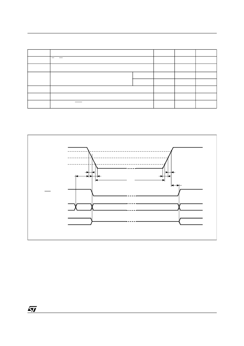
Table 8. Power Down/Up AC Characteristics
(T
A
= 0 to 70 °C or –40 to 85 °C)
Symbol
Note: 1. V
PFD
(max) to V
PFD
(min) fall time of less than t
F
may result in deselection/write protection not occurring until 200μs after V
CC
pass-
es V
PFD
(min).
2. V
PFD
(min) to V
SS
fall time of less than t
FB
may cause corruption of RAM data.
3. t
REC
(min) = 20ms for industrial temperature grade 6 device.
Parameter
Min
Max
Unit
t
PD
E or W at V
IH
before Power Down
0
μs
t
F
(1)
V
PFD
(max) to V
PFD
(min) V
CC
Fall Time
300
μs
t
FB
(2)
V
PFD
(min) to V
SS
V
CC
Fall Time
M48T59/Y
10
μs
M48T59V
150
μs
t
R
V
PFD
(min) to V
PFD
(max) V
CC
Rise Time
10
μs
t
RB
V
SS
to V
PFD
(min) V
CC
Rise Time
1
μs
t
REC
(3)
V
PFD
(max) to RST High
40
200
ms
Figure 5. Power Down/Up Mode AC Waveforms
AI03258
VCC
VPFD (max)
INPUTS
RST
OUTPUTS
DON'T CARE
HIGH-Z
tF
tFB
tR
tREC
tRB
tDR
VALID
VALID
VPFD (min)
VSO
tPD
RECOGNIZED
RECOGNIZED
(PER CONTROL INPUT)
(PER CONTROL INPUT)
The SOIC and battery/crystal packages are
shipped separately in plastic anti-static tubes or in
Tape & Reel form. For the 28 lead SOIC, the bat-
tery/crystal package (i.e. SNAPHAT) part number
is "M4T28-BR12SH" or “M4T32-BR12SH”.
Caution:
Do not place the SNAPHAT battery/crys-
tal top in conductive foam, as this will drain the lith-
ium button-cell battery.
As Figure 3 shows, the static memory array and
the quartz controlled clock oscillator of the
M48T59/59Y/59V are integrated on one silicon
chip.
The two circuits are interconnected at the upper
eight memory locations to provide user accessible
BYTEWIDE clock information in the bytes with
addresses 1FF8h-1FFFh. The clock locations
contain the century, year, month, date, day, hour,
minute, and second in 24 hour BCD format (except
for the century). Corrections for 28, 29 (leap year),
30, and 31 day months are made automatically.
Byte 1FF8h is the clock control register. This byte
controls user access to the clock information and
also stores the clock calibration setting.
相關(guān)PDF資料 |
PDF描述 |
|---|---|
| M48T59VPC | 64 Kbit 8Kb x8 TIMEKEEPER SRAM |
| M48T59VSH | 64 Kbit 8Kb x8 TIMEKEEPER SRAM |
| M48T59Y-70MH1 | 64 Kbit 8Kb x8 TIMEKEEPER SRAM |
| M48T59Y-70MH1TR | 64 Kbit 8Kb x8 TIMEKEEPER SRAM |
| M48T59Y-70PC1TR | 64 Kbit 8Kb x8 TIMEKEEPER SRAM |
相關(guān)代理商/技術(shù)參數(shù) |
參數(shù)描述 |
|---|---|
| M48T59MH | 制造商:STMICROELECTRONICS 制造商全稱:STMicroelectronics 功能描述:64 Kbit 8Kb x8 TIMEKEEPER SRAM |
| M48T59PC | 制造商:STMICROELECTRONICS 制造商全稱:STMicroelectronics 功能描述:64 Kbit 8Kb x8 TIMEKEEPER SRAM |
| M48T59SH | 制造商:STMICROELECTRONICS 制造商全稱:STMicroelectronics 功能描述:64 Kbit 8Kb x8 TIMEKEEPER SRAM |
| M48T59V | 制造商:STMICROELECTRONICS 制造商全稱:STMicroelectronics 功能描述:64 Kbit 8Kb x8 TIMEKEEPER SRAM |
| M48T59V-70MH1 | 制造商:STMICROELECTRONICS 制造商全稱:STMicroelectronics 功能描述:64 Kbit 8Kb x8 TIMEKEEPER SRAM |
發(fā)布緊急采購,3分鐘左右您將得到回復(fù)。