- 您現(xiàn)在的位置:買賣IC網(wǎng) > PDF目錄359067 > M48T59Y-70MH1 (意法半導體) 64 Kbit 8Kb x8 TIMEKEEPER SRAM PDF資料下載
參數(shù)資料
| 型號: | M48T59Y-70MH1 |
| 廠商: | 意法半導體 |
| 英文描述: | 64 Kbit 8Kb x8 TIMEKEEPER SRAM |
| 中文描述: | 64千位8KB的x8 SRAM的計時器 |
| 文件頁數(shù): | 9/17頁 |
| 文件大小: | 135K |
| 代理商: | M48T59Y-70MH1 |
The eight clock bytes are not the actual clock
counters themselves; they are memory locations
consisting of BiPORT
read/write memory cells.
The M48T58/58Y includes a clock control circuit
which updates the clock bytes with current informa-
tion once per second. The information can be
accessed by the user in the same manner as any
other location in the static memory array.
The M48T58/58Y also has its own Power-fail De-
tect circuit. The control circuitry constantly monitors
the single 5V supply for an out of tolerance condi-
tion. When V
CC
is out of tolerance, the circuit write
protects the SRAM, providing a high degree of data
security in the midst of unpredictable system op-
eration brought on by low V
CC
. As V
CC
falls below
approximately 3V, the control circuitry connects the
battery which maintains data and clock operation
until valid power returns.
READ MODE
The M48T58/58Y is in the Read Mode whenever
W (Write Enable) is high, E1 (Chip Enable 1) is low,
and E2 (Chip Enable 2) is high. The unique address
specified by the 13 Address Inputs defines which
one of the 8,192 bytes of data is to be accessed.
Valid data will be available at the Data I/O pins
within Address Access time (t
AVQV
) after the last
address input signal is stable, providing that the E1,
E2, and G access times are also satisfied. If the E1,
E2 and G access times are not met, valid data will
be available after the latter of the Chip Enable
Access times (t
E1LQV
or t
E2HQV
) or Output Enable
Access time (t
GLQV
).
The state of the eight three-state Data I/O signals
is controlled by E1, E2 and G. If the outputs are
activated before t
AVQV
, the data lines will be driven
to an indeterminate state until t
AVQV
. If the Address
Inputs are changed while E1, E2 and G remain
active, output data will remain valid for Output Data
Hold time (t
AXQX
) but will go indeterminate until the
next Address Access.
WRITE MODE
The M48T58/58Y is in the Write Mode whenever W
and E1 are low and E2 is high. The start of a write
is referenced from the latter occurring falling edge
of W or E1, or the rising edge of E2. A write is
terminated by the earlier rising edge of W or E1, or
the falling edge of E2. The addresses must be held
valid throughout the cycle. E1 or W must return high
or E2 low for a minimum of t
E1HAX
or t
E2LAX
from
Chip Enable or t
WHAX
from Write Enable prior to the
initiation of another read or write cycle. Data-in
must be valid t
DVWH
prior to the end of write and
remain valid for t
WHDX
afterward. G should be kept
high during write cycles to avoid bus contention;
although, if the output bus has been activated by a
low on E1 and G and a high on E2, a low on W will
disable the outputs t
WLQZ
after W falls.
DESCRIPTION
(cont’d)
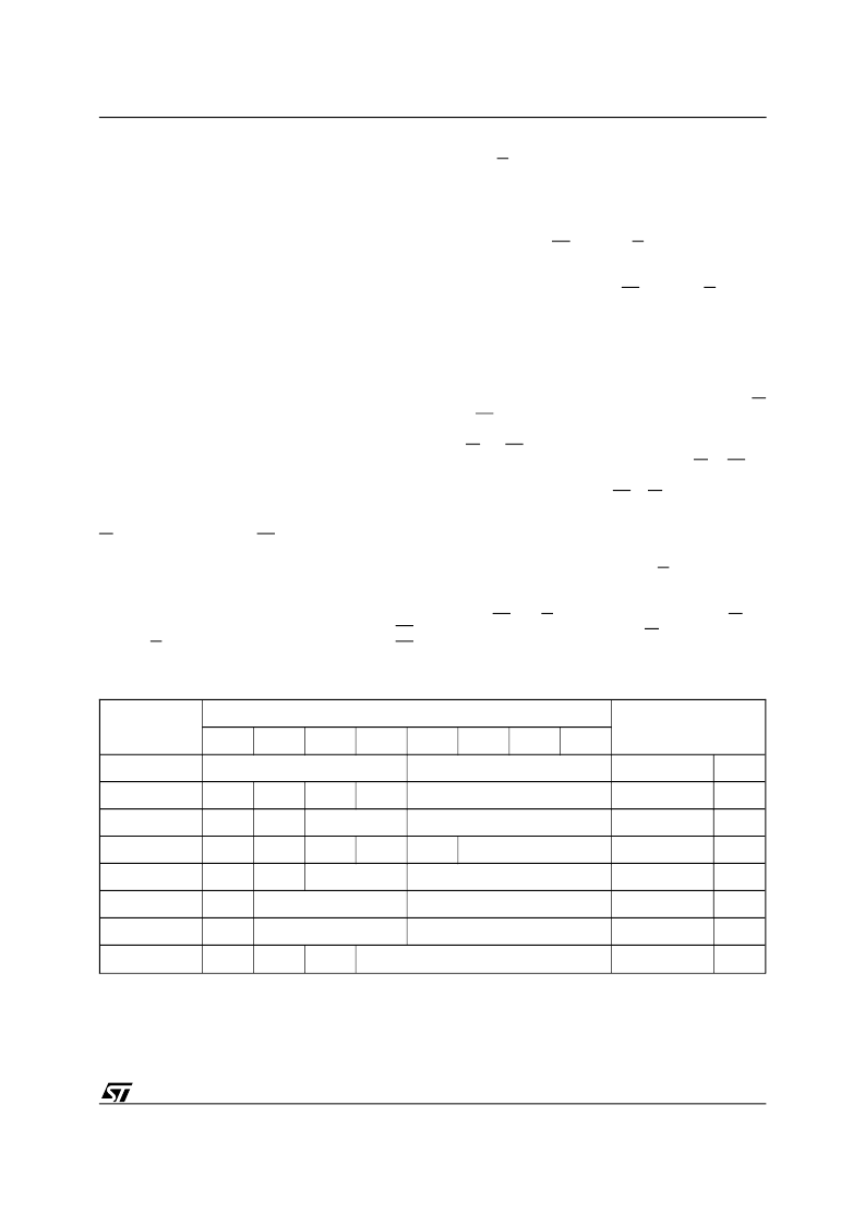
Address
Data
Function/Range
BCD Format
D7
D6
D5
D4
D3
D2
D1
D0
1FFFh
10 Years
Year
Year
00-99
1FFEh
0
0
0
10 M.
Month
Month
01-12
1FFDh
0
0
10 Date
Date
Date
01-31
1FFCh
0
FT
0
0
0
Day
Day
01-07
1FFBh
0
0
10 Hours
Hours
Hour
00-23
1FFAh
0
10 Minutes
Minutes
Minutes
00-59
1FF9h
ST
10 Seconds
Seconds
Seconds
00-59
1FF8h
W
R
S
Calibration
Control
Keys:
S = SIGN Bit
FT = FREQUENCY TEST Bit (Must be set to ’0’ upon power, for normal clock operation)
R = READ Bit
W = WRITE Bit
ST = STOP Bit
0 = Must be set to ’0’
Table 11. Register Map
9/17
M48T58, M48T58Y
相關(guān)PDF資料 |
PDF描述 |
|---|---|
| M48T59Y-70MH1TR | 64 Kbit 8Kb x8 TIMEKEEPER SRAM |
| M48T59Y-70PC1TR | 64 Kbit 8Kb x8 TIMEKEEPER SRAM |
| M48TMH1 | 5V PC REAL TIME CLOCK |
| M48TMH1TR | 5V PC REAL TIME CLOCK |
| M48TY-85MH1 | 3.3V-5V TIMEKEEPER CONTROLLER |
相關(guān)代理商/技術(shù)參數(shù) |
參數(shù)描述 |
|---|---|
| M48T59Y-70MH1E | 功能描述:實時時鐘 64K (8Kx8) 70ns RoHS:否 制造商:Microchip Technology 功能:Clock, Calendar. Alarm RTC 總線接口:I2C 日期格式:DW:DM:M:Y 時間格式:HH:MM:SS RTC 存儲容量:64 B 電源電壓-最大:5.5 V 電源電壓-最小:1.8 V 最大工作溫度:+ 85 C 最小工作溫度: 安裝風格:Through Hole 封裝 / 箱體:PDIP-8 封裝:Tube |
| M48T59Y-70MH1F | 功能描述:實時時鐘 64K (8Kx8) 70ns RoHS:否 制造商:Microchip Technology 功能:Clock, Calendar. Alarm RTC 總線接口:I2C 日期格式:DW:DM:M:Y 時間格式:HH:MM:SS RTC 存儲容量:64 B 電源電壓-最大:5.5 V 電源電壓-最小:1.8 V 最大工作溫度:+ 85 C 最小工作溫度: 安裝風格:Through Hole 封裝 / 箱體:PDIP-8 封裝:Tube |
| M48T59Y-70MH1TR | 制造商:STMICROELECTRONICS 制造商全稱:STMicroelectronics 功能描述:64 Kbit 8Kb x8 TIMEKEEPER SRAM |
| M48T59Y-70MH6 | 功能描述:實時時鐘 R 511-M48T59Y-70MH6E RoHS:否 制造商:Microchip Technology 功能:Clock, Calendar. Alarm RTC 總線接口:I2C 日期格式:DW:DM:M:Y 時間格式:HH:MM:SS RTC 存儲容量:64 B 電源電壓-最大:5.5 V 電源電壓-最小:1.8 V 最大工作溫度:+ 85 C 最小工作溫度: 安裝風格:Through Hole 封裝 / 箱體:PDIP-8 封裝:Tube |
| M48T59Y-70MH6E | 功能描述:實時時鐘 64K (8Kx8) 70ns RoHS:否 制造商:Microchip Technology 功能:Clock, Calendar. Alarm RTC 總線接口:I2C 日期格式:DW:DM:M:Y 時間格式:HH:MM:SS RTC 存儲容量:64 B 電源電壓-最大:5.5 V 電源電壓-最小:1.8 V 最大工作溫度:+ 85 C 最小工作溫度: 安裝風格:Through Hole 封裝 / 箱體:PDIP-8 封裝:Tube |
發(fā)布緊急采購,3分鐘左右您將得到回復(fù)。