- 您現(xiàn)在的位置:買賣IC網(wǎng) > PDF目錄370967 > M54974P (Mitsubishi Electric Corporation) Bi-CMOS 12-BIT SERIAL-INPUT LATCHED DRIVER PDF資料下載
參數(shù)資料
| 型號: | M54974P |
| 廠商: | Mitsubishi Electric Corporation |
| 英文描述: | Bi-CMOS 12-BIT SERIAL-INPUT LATCHED DRIVER |
| 中文描述: | 雙CMOS 12位串行輸入鎖存驅(qū)動 |
| 文件頁數(shù): | 1/6頁 |
| 文件大小: | 654K |
| 代理商: | M54974P |

Bi-CMOS 12-BIT SERIAL-INPUT LATCHED DRIVER
M54974P
MITSUBISHI <CONTROL / DRIVER IC>
DESCRIPTION
The M54974P is a semiconductor integrated circuit consisting of 12
stages of CMOS shift registers and latches with serial inputs and
serial or parallel outputs. It is based on Bi-CMOS process
technology, and has 12 bipolar drivers at the parallel outputs.
FEATURES
G
Serial input and serial or parallel output
G
Serial output enables cascade connection
G
Built-in latch for each stage
G
Enable input provides output control
G
Low supply current (standby current I
CC
≤
10
μ
A)
G
Serial I/O level is compatible with typical CMOS devices
G
Driver features: High withstand voltage (BV
CEO
≥
30V)
Capable of large drive currents (I
O(max)
=300mA)
G
Wide operating temperature range T
a
=-20 – +75
°
C
APPLICATION
Dot drivers for thermal print heads. Serial/parallel conversion.
Drivers for relay and solenoids.
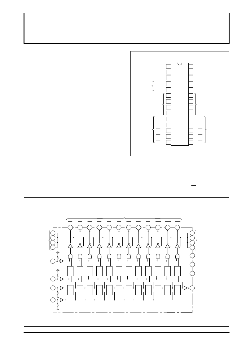
FUNCTION
The M54974P consists of 12 stages of D-type flip flops connected
to 12 latches.
Data is input to serial input S-IN, and clock pulses are applied to
clock input T. When the clock changes from low to high, the input
data enters the first shift register and data already in the shift
registers is shifted sequentially.
The serial output S-OUT is used to connect multiple M54974Ps to
expand the number of parallel outputs. S-OUT is connected to S-IN
of the next stage.
When the clock pulse changes from low to high, latch input
(LATCH) is high and output enable input (EN) is low the serial input
data at S-IN appears at output O1 and the other data already
BLOCK DIAGRAM
PIN CONFIGURATION (TOP VIEW)
Outline
28P4B
28
25
26
27
1
4
3
2
24
5
23
6
20
9
19
10
18
11
17
16
12
13
14
15
7
8
22
21
←
→
→
←
←
←
←
←
←
←
S-OUT
LATCH
EN
O12
O11
P-GND
O10
O9
O8
O7
O6
←
←
→
→
→
→
→
O5
O4
O3
O2
O1
P-GND
L-V
CC
L-GND
S-IN
T
P-V
CC
Serial output
Latch input
Enable input
Parallel outputs
Driver GND
Parallel outputs
Logic power
supply
Logic GND
Serial input
Clock
Output power
supply
Driver GND
Parallel outputs
M
P-V
Output power supply
Q
L D
O1
19
T
Clock
Q
T
D
8
9
3
2
26
25
Q
L D
O2
18
Q
T
D
Q
L D
O3
17
Q
T
D
Q
L D
O4
16
Q
T
D
Q
L D
O5
15
Q
T
D
Q
L D
O6
14
Q
T
D
Q
L D
O7
13
Q
T
D
Q
L D
O8
12
Q
T
D
Q
L D
O9
11
Q
T
D
Q
L D
O10
10
Q
T
D
Q
L D
O11
5
Q
T
D
Q
L D
O12
4
Q
T
D
1
20
21
22
23
24
23
27
EN
L-V
CC
L-V
CC
P-GND
Driver GND
S-OUT
Serial output
L-GND
Logic GND
L-V
CC
Logic power supply
Parallel outputs
6
7
Driver GND
P-GND
Latch input
LATCH
Serial input
S-IN
Enable input
相關(guān)PDF資料 |
PDF描述 |
|---|---|
| M54975 | Bi-CMOS 8-BIT SERIAL-INPUT LATCHED DRIVER |
| M54975FP | Bi-CMOS 8-BIT SERIAL-INPUT LATCHED DRIVER |
| M54975P | Bi-CMOS 8-BIT SERIAL-INPUT LATCHED DRIVER |
| M54977 | Bi-CMOS 12-BIT SERIAL-INPUT LATCHED DRIVER |
| M54977P | Bi-CMOS 12-BIT SERIAL-INPUT LATCHED DRIVER |
相關(guān)代理商/技術(shù)參數(shù) |
參數(shù)描述 |
|---|---|
| M54975 | 制造商:MITSUBISHI 制造商全稱:Mitsubishi Electric Semiconductor 功能描述:Bi-CMOS 8-BIT SERIAL-INPUT LATCHED DRIVER |
| M54975FP | 制造商:MITSUBISHI 制造商全稱:Mitsubishi Electric Semiconductor 功能描述:Bi-CMOS 8-BIT SERIAL-INPUT LATCHED DRIVER |
| M54975P | 制造商:MITSUBISHI 制造商全稱:Mitsubishi Electric Semiconductor 功能描述:Bi-CMOS 8-BIT SERIAL-INPUT LATCHED DRIVER |
| M54977 | 制造商:MITSUBISHI 制造商全稱:Mitsubishi Electric Semiconductor 功能描述:Bi-CMOS 12-BIT SERIAL-INPUT LATCHED DRIVER |
| M54977P | 制造商:MITSUBISHI 制造商全稱:Mitsubishi Electric Semiconductor 功能描述:Bi-CMOS 12-BIT SERIAL-INPUT LATCHED DRIVER |
發(fā)布緊急采購,3分鐘左右您將得到回復(fù)。