- 您現(xiàn)在的位置:買賣IC網(wǎng) > PDF目錄224150 > M5913 (意法半導(dǎo)體) COMBINED SINGLE CHIP PCM CODEC AND FILTER PDF資料下載
參數(shù)資料
| 型號(hào): | M5913 |
| 廠商: | 意法半導(dǎo)體 |
| 元件分類: | Codec |
| 英文描述: | COMBINED SINGLE CHIP PCM CODEC AND FILTER |
| 中文描述: | 組合單芯片的PCM編解碼器和過(guò)濾器 |
| 文件頁(yè)數(shù): | 11/17頁(yè) |
| 文件大?。?/td> | 220K |
| 代理商: | M5913 |
第1頁(yè)第2頁(yè)第3頁(yè)第4頁(yè)第5頁(yè)第6頁(yè)第7頁(yè)第8頁(yè)第9頁(yè)第10頁(yè)當(dāng)前第11頁(yè)第12頁(yè)第13頁(yè)第14頁(yè)第15頁(yè)第16頁(yè)第17頁(yè)
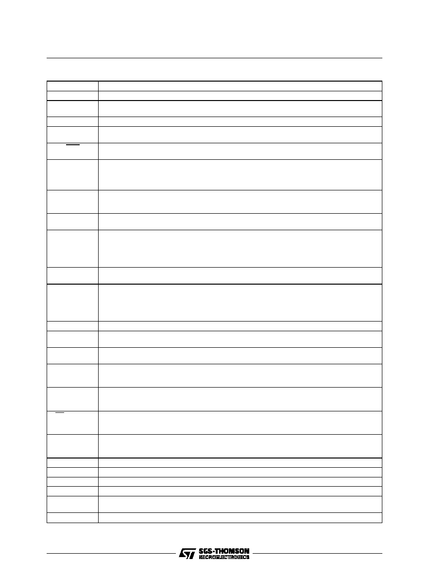
PIN DESCRIPTION
Symbol
Function
VBB
Most Negative Supply. Input voltage is -5 volts
±5%.
PWRO+
Non-inverting Output of Power Amplifier. Can drive transformer hybrids or high impedance loads
directly in either a differential or single ended configuration.
PWRO -
Inverting Output of Power Amplifier. Functionally identical and complementary to PWRO+.
GSR
Input to the gain Setting Network on the Output Power Amplifier, Transmission level can be
adjusted over a 12dB range depending on the voltage at GSR.
PDN
Power Down Select. When PDN is TTL high, the device is active.When low, the device is powered
down.
CLKSEL
input which must be pinstrapped to reflect the master clock frequency at CLKX, CLKR.
CLKSEL = VBB
2.048MHz
CLKSEL = GRDD
1.544MHz
CLKSEL = VCC
1.536MHz
LOOP
Analog Loopback. When this pin is TTL high, the receive output (PWRO+) is internally connected
to VFXI+, GSR is internally connected to PWRO-, and VFXI- is internally connected to GSX.
A 0dBm0 digital signal input at DR is returned as a +3dBm0 digital signal output at DX.
SIGR
Signalling Bit Output, Receive Channel. In fixed data rate mode. SIGR outputs the logical state of
the eighth bit of the PCM word in the most recent signaling frame.
DCLKR
Selects the fixed or variable data rate mode. When DCLKR is connected to VBB, the fixed data rate
mode is selected.
When DCLKR is not connected to VBB, the device operates in the variable data rate mode. In this
mode DCLKR becomes the receive data clock wich operates at TTL levels from 64kB to 4.096MB
data rates
DR
Receive PCM Input. PCM data is clocked in on this lead on eight consecutive negative transitions
of the receive data clock: CLKR in the fixed data rate mode and DCLKR in variable data rate mode.
FSR
8kHz frame synchronization clock input/timeslot enable, receive channel. A multifunction input
which in fixed data rate mode distinguishes between signaling and non-signaling frames by means
of a double or single wide pulse respectively. In variable data rate mode this signal must remain
high for the entire length of the timeslot. The receive channel enters the standby state whenever
FSR is TTL low for 30 miliseconds
GRDD
Digital Ground for all Internal Logic Circuits. Not internally tied to GRDA.
CLKR
Receive master and data clock for the fixed data rate mode; receive master clock only in variable
data rate mode.
CLKX
Transmit master and data clock for the fixed data rate mode; transmit master clock only in variable
data rate mode.
FSX
8kHz frame synchronization clock input/timeslot enable, transmit channel. Operates independently
but in an analogous manner to FSR. The transmit channel enters the standby state whenever FSX
is TTL low for 30 milliseconds.
DX
Transmit PCM Output. PCM data is clocked out on this lead on eight consecutive positive
transitions of the transmit data clock : CLK in fixed data rate mode and DCLKX in variable data rate
mode.
TSX/DCLKX
Transmit channel timeslot strobe (output) or data clock (input) for the transmit channel. In fixed
data rate mode, this pin becomes the transmit data clock which operates at TTL levels from 64kB
to 4.096MB data rates.
SIGX/ASEL
A dual purpose selects
-law and pin. When connected to VBB. A law operation is selected. When it
is not connected to VBB pin is a TTL level input for signaling operation. This input is transmitted as
the eighth bit of the PCM word during signaling frames on the DX lead.
NC
Not Connected.
GRDA
Analog ground return for all internal voice circuits. Not internally connected to GRDD.
VFXI+
Non inverting analog input to uncommitted transmit operational amplifier.
VFXI-
Inverting analog input to uncommitted transmit operational amplifier.
GSX
Output terminal of on-chip uncommitted op amp. Internally, this is the voice signal input to the
transmit filter.
VCC
Most positive supply ; input voltage is + 5 volts
±5%
M5913
3/17
相關(guān)PDF資料 |
PDF描述 |
|---|---|
| M5913B1 | COMBINED SINGLE CHIP PCM CODEC AND FILTER |
| M5F78M05 | 5 V FIXED POSITIVE REGULATOR, PSFM3 |
| M5F78M06 | 6 V FIXED POSITIVE REGULATOR, PSFM3 |
| M5F78M08 | 8 V FIXED POSITIVE REGULATOR, PSFM3 |
| M5F78M09 | 9 V FIXED POSITIVE REGULATOR, PSFM3 |
相關(guān)代理商/技術(shù)參數(shù) |
參數(shù)描述 |
|---|---|
| M5913B1 | 制造商:STMICROELECTRONICS 制造商全稱:STMicroelectronics 功能描述:COMBINED SINGLE CHIP PCM CODEC AND FILTER |
| M5917 | 制造商:Madison Company 功能描述:Max Temperature 250 C, SS Float, Bulk |
| M5920025-AL | 制造商:OKW ENCLOSURES INC 功能描述:Enclosure;Cabinet;Rackmount;Aluminum;Gray;19In,2U,10.351InDepth;MettecSeries |
| M5920035-AL | 制造商:OKW ENCLOSURES INC 功能描述:Enclosure;Cabinet;Rackmount;Aluminum;Gray;19In,2U,14.469InDepth;MettecSeries |
| M5930025-AL | 制造商:OKW ENCLOSURES INC 功能描述:Enclosure;Cabinet;Rackmount;Aluminum;Gray;19In,3U,10.351InDepth;MettecSeries |
發(fā)布緊急采購(gòu),3分鐘左右您將得到回復(fù)。