- 您現(xiàn)在的位置:買賣IC網(wǎng) > PDF目錄180240 > M7A3P400-FFGG256 FPGA, 400000 GATES, 350 MHz, PBGA256 PDF資料下載
參數(shù)資料
| 型號: | M7A3P400-FFGG256 |
| 元件分類: | FPGA |
| 英文描述: | FPGA, 400000 GATES, 350 MHz, PBGA256 |
| 封裝: | 1 MM PITCH, GREEN, FBGA-256 |
| 文件頁數(shù): | 218/246頁 |
| 文件大?。?/td> | 3010K |
| 代理商: | M7A3P400-FFGG256 |
第1頁第2頁第3頁第4頁第5頁第6頁第7頁第8頁第9頁第10頁第11頁第12頁第13頁第14頁第15頁第16頁第17頁第18頁第19頁第20頁第21頁第22頁第23頁第24頁第25頁第26頁第27頁第28頁第29頁第30頁第31頁第32頁第33頁第34頁第35頁第36頁第37頁第38頁第39頁第40頁第41頁第42頁第43頁第44頁第45頁第46頁第47頁第48頁第49頁第50頁第51頁第52頁第53頁第54頁第55頁第56頁第57頁第58頁第59頁第60頁第61頁第62頁第63頁第64頁第65頁第66頁第67頁第68頁第69頁第70頁第71頁第72頁第73頁第74頁第75頁第76頁第77頁第78頁第79頁第80頁第81頁第82頁第83頁第84頁第85頁第86頁第87頁第88頁第89頁第90頁第91頁第92頁第93頁第94頁第95頁第96頁第97頁第98頁第99頁第100頁第101頁第102頁第103頁第104頁第105頁第106頁第107頁第108頁第109頁第110頁第111頁第112頁第113頁第114頁第115頁第116頁第117頁第118頁第119頁第120頁第121頁第122頁第123頁第124頁第125頁第126頁第127頁第128頁第129頁第130頁第131頁第132頁第133頁第134頁第135頁第136頁第137頁第138頁第139頁第140頁第141頁第142頁第143頁第144頁第145頁第146頁第147頁第148頁第149頁第150頁第151頁第152頁第153頁第154頁第155頁第156頁第157頁第158頁第159頁第160頁第161頁第162頁第163頁第164頁第165頁第166頁第167頁第168頁第169頁第170頁第171頁第172頁第173頁第174頁第175頁第176頁第177頁第178頁第179頁第180頁第181頁第182頁第183頁第184頁第185頁第186頁第187頁第188頁第189頁第190頁第191頁第192頁第193頁第194頁第195頁第196頁第197頁第198頁第199頁第200頁第201頁第202頁第203頁第204頁第205頁第206頁第207頁第208頁第209頁第210頁第211頁第212頁第213頁第214頁第215頁第216頁第217頁當(dāng)前第218頁第219頁第220頁第221頁第222頁第223頁第224頁第225頁第226頁第227頁第228頁第229頁第230頁第231頁第232頁第233頁第234頁第235頁第236頁第237頁第238頁第239頁第240頁第241頁第242頁第243頁第244頁第245頁第246頁
ProASIC3 Flash Family FPGAs
v2.1
3-3
I/O Power-Up and Supply Voltage Thresholds for Power-On Reset (Commercial and
Industrial)
Sophisticated
power-up
management
circuitry
is
designed into every ProASIC3 device. These circuits
ensure easy transition from the powered-off state to the
powered-up state of the device. The many different
supplies can power up in any sequence with minimized
current spikes or surges. In addition, the I/O will be in a
known state through the power-up sequence. The basic
principle is shown in Figure 3-1.
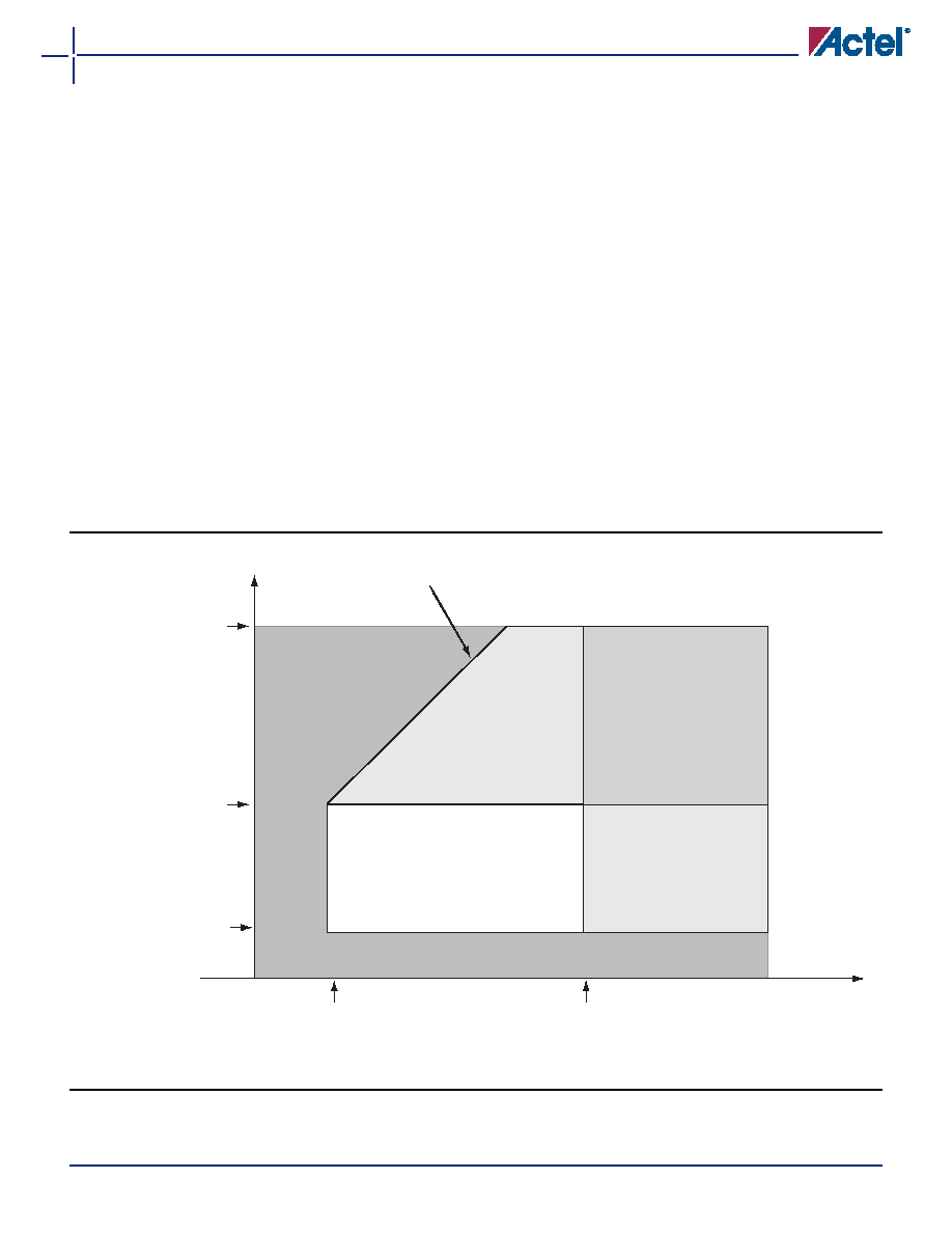
There are five regions to consider during power-up.
ProASIC3 I/Os are activated only if ALL of the following
three conditions are met:
1. VCC and VCCI are above the minimum specified trip
points (Figure 3-1).
2. VCCI > VCC – 0.75 V (typical)
3. Chip is in the operating mode.
VCCI Trip Point:
Ramping up: 0.6 V < trip_point_up < 1.2 V
Ramping down: 0.5 V < trip_point_down < 1.1 V
VCC Trip Point:
Ramping up: 0.6 V < trip_point_up < 1.1 V
Ramping down: 0.5 V < trip_point_down < 1 V
VCC and VCCI ramp-up trip points are about 100 mV
higher than ramp-down trip points. This specifically
built-in
hysteresis
prevents
undesirable
power-up
oscillations and current surges. Note the following:
During programming, I/Os become tristated and
weakly pulled up to VCCI.
JTAG supply, PLL power supplies, and charge pump
VPUMP supply have no influence on I/O behavior.
Internal Power-Up Activation Sequence
1. Core
2. Input buffers
3. Output buffers, after 200 ns delay from input
buffer activation
Figure 3-1
I/O State as a Function of VCCI and VCC Voltage Levels
Region 1: I/O buffers are OFF
Region 2: I/O buffers are ON.
I/Os are functional (except differential inputs)
but slower because V
CCI
/V
CC
are below
specification. For the same reason, input
buffers do not meet V
IH
/V
IL
levels, and
output buffers do not meet V
OH
/V
OL
levels.
Min V
CCI datasheet specification
voltage at a selected I/O
standard; i.e., 1.425 V or 1.7 V
or 2.3 V or 3.0 V
VCC
VCC = 1.425 V
Region 1: I/O Buffers are OFF
Activation trip point:
Va = 0.85 V ± 0.25 V
Deactivation trip point:
Vd = 0.75 V ± 0.25 V
Activation trip point:
Va = 0.9 V ± 0.3 V
Deactivation trip point:
Vd = 0.8 V ± 0.3 V
VCC = 1.575 V
Region 5: I/O buffers are ON
and power supplies are within
specification.
I/Os meet the entire datasheet
and timer specifications for
speed, V
IH
/V
IL
, V
OH
/V
OL
, etc.
Region 4: I/O
buffers are ON.
I/Os are functional
(except differential
but slower because V
CCI is
below specification. For the
same reason, input buffers do not
meet V
IH
/V
IL
levels, and output
buffers do not meet V
OH
/V
OL
levels.
Region 4: I/O
buffers are ON.
I/Os are functional
(except differential inputs)
where VT can be from 0.58 V to 0.9 V (typically 0.75 V)
VCCI
Region 3: I/O buffers are ON.
I/Os are functional; I/O DC
specifications are met,
but I/Os are slower because
the V
CC
is below specification.
V
CC = VCCI + VT
相關(guān)PDF資料 |
PDF描述 |
|---|---|
| M7A3P400-FFGG484 | FPGA, 400000 GATES, 350 MHz, PBGA484 |
| M7A3P400-FG144I | FPGA, 400000 GATES, 350 MHz, PBGA144 |
| M7A3P400-FG144 | FPGA, 400000 GATES, 350 MHz, PBGA144 |
| M7A3P400-FG256I | FPGA, 400000 GATES, 350 MHz, PBGA256 |
| M7A3P400-FG256 | FPGA, 400000 GATES, 350 MHz, PBGA256 |
相關(guān)代理商/技術(shù)參數(shù) |
參數(shù)描述 |
|---|---|
| M7A5 | 制造商:未知廠家 制造商全稱:未知廠家 功能描述:MEDIUM CURRENT SILICON RECTIFIERS |
| M7A9 | 制造商:未知廠家 制造商全稱:未知廠家 功能描述:MEDIUM CURRENT SILICON RECTIFIERS |
| M7AFS600-1FG256 | 制造商:Microsemi Corporation 功能描述:FPGA FUSION 600K GATES 1282.05MHZ 130NM 1.5V 256FBGA - Trays 制造商:Microsemi SOC Products Group 功能描述:FPGA FUSION 600K GATES 1282.05MHZ 130NM 1.5V 256FBGA - Trays |
| M7AFS600-1FG256ES | 制造商:ACTEL 制造商全稱:Actel Corporation 功能描述:Actel Fusion Mixed-Signal FPGAs |
| M7AFS600-1FG256I | 制造商:Microsemi Corporation 功能描述:FPGA FUSION 600K GATES 1282.05MHZ 130NM 1.5V 256FBGA - Trays 制造商:Microsemi SOC Products Group 功能描述:FPGA FUSION 600K GATES 1282.05MHZ 130NM 1.5V 256FBGA - Trays |
發(fā)布緊急采購,3分鐘左右您將得到回復(fù)。