- 您現(xiàn)在的位置:買賣IC網(wǎng) > PDF目錄359125 > MA4SPS502 Surface Mount Monolithic PIN Diode Chip PDF資料下載
參數(shù)資料
| 型號(hào): | MA4SPS502 |
| 英文描述: | Surface Mount Monolithic PIN Diode Chip |
| 中文描述: | 表面貼裝芯片單片PIN二極管 |
| 文件頁(yè)數(shù): | 2/3頁(yè) |
| 文件大小: | 126K |
| 代理商: | MA4SPS502 |

Surface Mount Monolithic PIN Diode Chip
MA4SPS502 SurMount
TM
Series
Specifications subject to change without notice.
n
North America:
Tel. (800) 366-2266
n
Asia/Pacific:
Tel.+81-44-844-8296, Fax +81-44-844-8298
n
Europe:
Tel. +44 (1344) 869 595, Fax+44 (1344) 300 020
Visit www.macom.com for additional data sheets and product information.
Electrical Specifications: @ 25 °C
Symbol
Test Conditions
Units
Min.
Typ.
Max.
C
T
-40 Volts, 1 MHz
pF
0.140
0.200
C
T
-40 Volts, 1 GHz
pF
0.090
R
S
100 mA, 100 MHz
1.4
R
S
20 mA, 100 MHz
2.4
V
F
100 mA
V
1.24
1.50
V
F
10 mA
V
0.87
1.00
V
R
10
μ
A
V
-300
-330
I
R
-300 V
μ
A
10
I
R
-40 V
nA
8
R
θ
JL
Steady state
°C/W
75
T
L
+10 mA / -6 mA measured at 90% voltage
μs
2.8
2
Handling Procedures
All semiconductor chips should be handled with care to avoid
damage or contamination from perspiration and skin oils. The
use of plastic tipped tweezers or vacuum pickups is strongly
recommended for individual components. Bulk handling should
insure that abrasion and mechanical shock are minimized.
Bonding Techniques
Attachment to a circuit board is made simple through the use of
surface mount technology. Mounting pads are conveniently
located on the bottom surface of these diodes and are removed
from the active junction locations. These devices are well suited
for solder attachment onto hard and soft substrates. The use of
80/20 Au/Sn and 60/40 Sn/Pb solder is recommended, with an
equal temperature profile across the contacts. Conductive epoxy
paste for attachment may also be used.
When soldering these devices to a hard substrate, hot gas die
bonding is preferred. We recommend utilizing a vacuum tip and
a force of 60 to 100 grams applied normal to the top surface of
the device. When soldering to soft substrates, it is recommended
to use a lead-tin interface at the circuit board mounting pads.
Position the die so that its mounting pads are aligned with the
circuit board’s mounting pads and reflow the solder by heating
the circuit trace near the mounting pad while applying 60 to 100
grams of force perpendicular to the top surface of the die.
Since the HMIC glass is transparent, the edges of the mounting
pads closest to each other can be visually inspected through the
die after attach is completed.
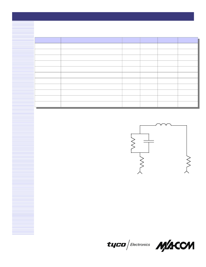
Functional Schematic
1
Rp
Cp
Ls
Rvia
Rvia
+
-
1. Rs = 2 * Rvia + Rp
相關(guān)PDF資料 |
PDF描述 |
|---|---|
| MA4SW424B-1 | Monolithic SP4T PIN Diode Switch With Integrated Bias Network |
| MA4VAT904-1061T | High IIP3 PIN Diode Variable Attenuator (0.80-1.0 GHz) |
| MA505 | ECM Surface Mount Crystal |
| MA838 | SINGLE PHASE PULSE WIDTH MODULATION WAVEFORM GENERATOR |
| MAADSS0010 | Digital Attenuator, 5-Bit, 31 dB (400 - 2500 MHz) |
相關(guān)代理商/技術(shù)參數(shù) |
參數(shù)描述 |
|---|---|
| MA4SPS502_1 | 制造商:MA-COM 制造商全稱:M/A-COM Technology Solutions, Inc. 功能描述:SURMOUNT PIN Diode |
| MA4SPS502-T | 制造商:M/A-COM Technology Solutions 功能描述:SURMOUNT PIN DIODE - LOW RC PRODUCT - Tape and Reel |
| MA4SPS552 | 制造商:M/A-COM Technology Solutions 功能描述:SURFACE MOUNT MONOLITHIC PIN DIODE CHIP - Gel-pak, waffle pack, wafer, diced wafer on film 制造商:M/A-COM Technology Solutions 功能描述:Diode PIN Attenuator/Switch 200V Die |
| MA4SPS552-T | 制造商:MA-COM 制造商全稱:M/A-COM Technology Solutions, Inc. 功能描述:SURMOUNTTM PIN Diode |
| MA4SPS552-W | 制造商:MA-COM 制造商全稱:M/A-COM Technology Solutions, Inc. 功能描述:SURMOUNTTM PIN Diode |
發(fā)布緊急采購(gòu),3分鐘左右您將得到回復(fù)。